Phono Stage - Open Loop Bandwidth
Hi all,
the simulation shows that the open loop bandwidth of phono stage jumps from 1kHz to 15kHz if we instead connect the bottom side of R10 (10 ohm) to the collector of the transistor on the right side, we connect to the collector of the transistor on the left of the second stage.
Please, refer to post #174
There is a tip only!
eD
Last edited:
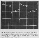
The square wave response looks perfect I would say. BTW, what values did you exactly use, I would be interested to see the schematic. And did you build the phono stage too ?
Hi gk7
I use the exact values of the attached schematic but changed R16/R18 to 150 Ohm.
I did build the phono stage but I have problem with the offset. I got 250mv at the output. Attached is the phono schematic I use.
Attachments
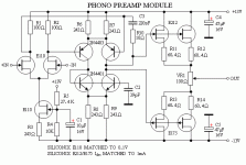
I think the connection between R8 and R9 should be removed (John said so, although he said it would work either way.) I suppose you used Toshiba FETs instead of the Fairchild in the schematics. What is the current through the input FETs (voltage across R1 or R2) ? I think the current source would need some adjustment. Did you try to lower the values for R11 to R14 ? I would lower R11 to R14 to 20R each and VR1 to 50R as a start. But I did not try that yet - just an idea.
Hi all,
the simulation shows that the open loop bandwidth of phono stage jumps from 1kHz to 15kHz if we instead connect the bottom side of R10 (10 ohm) to the collector of the transistor on the right side, we connect to the collector of the transistor on the left of the second stage.
Please, refer to post #174
There is a tip only!
eD
Post #174 was about removing the connection between R8 and R9 and thus making it a normal current mirror (which was originally intended I think). I´m a bit confused now, you suggest to connect the compensation network to the left transitors collector or to both collectors (which means leaving the connection betweenn R8 and R9 in place) ? Increasing the open loop bandwidth from 1kHz to 15kHz sounds a lot to me, in your simulation this was still stable ?
Perfect , isn't there 2 much tilt on the low freq response , the 1 k response looks right , the others not so sure ...
The slight tilt is normal for a capacitor coupled circuit. Attached is the square wave measurement from Audio magazine (April 1976) made of an original JC-2.
Attachments
Post #174 was about removing the connection between R8 and R9 and thus making it a normal current mirror (which was originally intended I think). I´m a bit confused now, you suggest to connect the compensation network to the left transitors collector or to both collectors (which means leaving the connection betweenn R8 and R9 in place) ? Increasing the open loop bandwidth from 1kHz to 15kHz sounds a lot to me, in your simulation this was still stable ?
Hi,
no both collectors. Instead to connect to right side, you may to connect to left side only - no problem with stability !
Can you tell to us about sound with and without that modification ?
If you want I can show some results and schematic that I used for it.
eD
Hi,
no both collectors. Instead to connect to right side, you may to connect to left side only - no problem with stability !
Can you tell to us about sound with and without that modification ?
If you want I can show some results and schematic that I used for it.
eD
Hi I am getting J74V/K170V for this build, can you send me the actual circuit and values - also any idea of the pcb ? would be great.
thanks- youcan PM me or email kannan_srinvasa at yahoo dot com
kannan
Hi I am getting J74V/K170V for this build, can you send me the actual circuit and values - also any idea of the pcb ? would be great.
thanks- youcan PM me or email kannan_srinvasa at yahoo dot com
kannan
Hi Kannan,
I had simulated the phono stage only and I used the 2SK369 fets in the diferential input and J175/J212 fets as output.
Besides this, I had take emitters connection ( both ) off from second stage as post # 174.
No pcb yet..sorry!
regardds
eD
Hi Kannan,
I had simulated the phono stage only and I used the 2SK369 fets in the diferential input and J175/J212 fets as output.
Besides this, I had take emitters connection ( both ) off from second stage as post # 174.
No pcb yet..sorry!
regardds
eD
Don´t take it personal but this sounds more like "circuit design by trial and error to me".
I doubt that you can "better" the original circuit by deliberately changing it.
What is the rationale behind this changes ?
As for stability: The circuit has to be unity gain stable and be able to drive capacitive loads, did you build it and checked stability with a high speed scope or are you solely relying on
simulations ?
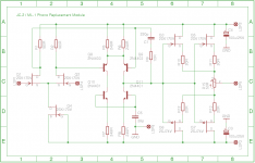
This is a (very) preliminary schematic of the phono circuit,
like I would build it with modern parts.
Changes to the original circuit are a simplified current source
(I think with the Toshiba FETs this can be done this way without
drawbacks I´m aware off - but comments welcome of course),
slightly increased R1 and R2 to make up for the lower current to
the Toshiba Fets, and resistors for the output source followers
adjusted as mentioned in post #205.
Attachments
Don´t take it personal but this sounds more like "circuit design by trial and error to me".
I doubt that you can "better" the original circuit by deliberately changing it.
What is the rationale behind this changes ?
As for stability: The circuit has to be unity gain stable and be able to drive capacitive loads, did you build it and checked stability with a high speed scope or are you solely relying on
simulations ?
I just suggested a tip for you when trying to build its version and tell us if it gets better or not. Just a suggestion. Everything else remains the same as the original. So if you do not want to try this tip, just forget it. My intention here was just TRY to improve since you will build because I will not. I think that other members here would like to know if that tip will to work or not.
regards
eD
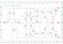
Hi gk7,
You may try this:
eD
How and why do you think this would this improve on the original design ? Especially the compensation (C1, R9) - I don´t think one can deliberately connect the compensation to some other point and expect this to do any good.
It _might_ work, but I still don´t see why it should work better (if it does at all).
It will be significantly noisier.
Hi John,
the simulation shows this significantly increase noise level with that modification but just without riaa correction. With riaa correction the noise is almost the same.
Do you agree ?
regards
eD
")
- Home
- Source & Line
- Analog Line Level
- Need to build JC 2 preamp