This is very interesting for several reasons, first the current consupmtion
(or is this the output stage bias ?)of the line module is much lower than expected.
John gave an overview for the "genealogy" of this circuit in Post #138, and also told us that
it´s not only about the absolute value of the BJT current but about
choosing the point with highest beta and ft. (For the BJTs I will use
this is in the 30-50mA range).
Another thing is the fairly high offset. (Meanwhile I have read the
second pot in my later modules is for offset adjustment - I will
measure it next weekend and also have a look how much it drifts).
This leads me to one of the suggestions from the Positive Feedback
article, the replacement of C18 by wire (schematic from Post #79).
Inside the Module there is a 4.7 MOhms feedback resistor (Post #19).
Thus with C18 in place DC gain is always 1 while AC gain is
set by VR5 + R34 in parallell and R33. With C18 replaced by wire, DC gain
will be the same as AC gain. This lead to much higher offset on the output
and it will vary when one operates VR5, which might be audible.
(I will test it next weekend).
A servo would proably be best to resolve the whole "capacitor issue",
but on the module area space is very limited.
Got the following information about the phono stage from Rolv-Karsten Ronningstad at marklev.com:
I am pretty sure that the connection between the emitters of the 2N4401 and the 2N4403 transistors in the second stage of the "phono" module should be removed.
Would anyone give comment for this?
I am pretty sure that the connection between the emitters of the 2N4401 and the 2N4403 transistors in the second stage of the "phono" module should be removed.
Would anyone give comment for this?
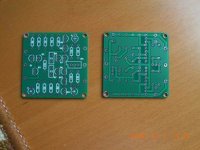
Attachments
john curl said:You are correct.
Hi John
Thank you for your comment. I am in soldering process and hopefully will be completed the phono stage in the next few days. I will keep up-dated.
Really for the 2N4401 _and_ the 2N4403s ?
For the two 2N4401 which form a current mirror this is clear, the connection between their emitters is wrong and must be removed.
But the two 2N4403 form a differential amplifier, which they would not be anymore if you disconnect their emitters.
I´m pretty sure that only the connection between the emittors of the 2N4401s (current mirror) should be removed, other than that the schematic is correct.
john curl said:Either way, or both would still work.
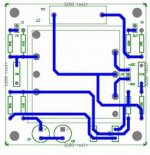
Which variant was choosen in the original circuit, this one:
Attachments

Hi guys happy Easter
I finished soldering the phono stage this morning. I got the following measurements across resistors. I changed value of R1 & R2 from 100 Ohm to 620 Ohm due to JFets idss. Other resistors values remain unchanged.
idss currents of the JFets are as follow:
Q1/Q2: 5ma
Q3: 9.5ma
Q8/Q9: 5.5ma
Q10/Q11: 5.5ma
R1: 620 Ohm = 3.5v
R2: 620 Ohm = 3.5v
R3: 243 Ohm = 2.8v
R4: 10K = 3.3v
R5: 27.4K = 0.01v
R6: 243 Ohm = 3.2v
R7: 243 Ohm = 3.1v
R8: 243 Ohm = 3.1v
R9: 243 Ohm = 3.1v
R10: 10 Ohm = 0v
R11: 60.4 Ohm = 0.2v
R12: 60.4 Ohm = 0.2v
R13: 60.4 Ohm = 0.2v
R14: 60.4 Ohm = 0.2v
Output offset = 0.022v
Comments are welcome.
Thanks
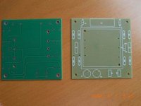
Attachments
Some voltages across resistors have been changed after 30 minutes run in:
R1 = 4.8v
R2 = 4.8v
R3 = 3.8v
R4 = 4.6v
R5 = 0.015v
R6 = 4.15v
R7 = 4.15v
R8 = 4.1v
R9 = 4.1v
R10 = 0v
R11 = 0.2v
R12 = 0.2v
R13 = 0.2v
R14 = 0.2v
Output = 0.9v I can not go lower by adjust the 100 Ohm VR
Please comment
R1 = 4.8v
R2 = 4.8v
R3 = 3.8v
R4 = 4.6v
R5 = 0.015v
R6 = 4.15v
R7 = 4.15v
R8 = 4.1v
R9 = 4.1v
R10 = 0v
R11 = 0.2v
R12 = 0.2v
R13 = 0.2v
R14 = 0.2v
Output = 0.9v I can not go lower by adjust the 100 Ohm VR
Please comment
Phono Module Offset
On my two Phono Modules (ML-1) I have measured this offset voltages:
about 10s after turn on: 87 mV and -24 mV
about 10 min. after turn on: 84 mV and -23 mV
In short: not much drift over time but substantially lower than the values you have. How close have you matched the input FETs ?
BTW, offset voltages for the line modules are 2.6 mV and 8 mV (after 10 sec.) and 2.3 mV and 3.7 mV (after 10 min.). (They have a DC gain of 1 due to C18 and an offset adjustment pot).
- Home
- Source & Line
- Analog Line Level
- Need to build JC 2 preamp