Final lot of GB boards
OK, looks like everyone that paid has their boards. I have ~15 stereo pairs left. $28 per pair + $4.60USA\11.00 ROTW shipping. Paypal bobgroger_at_hotmail_dot_com. All proceeds except shipping donated to DiyA.
OK, looks like everyone that paid has their boards. I have ~15 stereo pairs left. $28 per pair + $4.60USA\11.00 ROTW shipping. Paypal bobgroger_at_hotmail_dot_com. All proceeds except shipping donated to DiyA.
Re: PCB Projects,
there's only 7500 posts to read through.suds said:
Need schematic
Hey all, finally got my crap together and have the outputs and driver boards for one channel all connected.
I wired up my handy +/- 26VDC power supply to the driver/inputs and all is good (no smoke). I dialed in bias to get 1.2V across the driver resistors as indicated on the wiki. I then check the voltage across the output resistors and I can only get up to .025v. No matter how much I turn up the 5k bias trimpot, it maxes out at 1.5V on the driver resistors and .025 on the outputs resistors...the fets/sink does not even get warm...
I am not using my intended +/- 37V supply, as I wanted to check it with a lower supply first...could it be the lowish voltage/current from my test supply?
I was getting some values close to those on the wiki, but thought since I was at 27V rails and not 37V, I would be a bit off anyway....
Oh, and I have .649 ohm 10W output resistors and the outputs transistors are 2SA1943/2SC5200...
I have hooked up the +/- 40V supply and get these values almost exactly - from the wiki...
If your front end is working like mine you will get the following voltages:
r103, r107 (rail-0.6v)
r108, r109 (rail-27v)
r112, r113, r116, r117 ~2.2v
r120, r121 ~1.59v
r122, r123 ~1v
(voltages measured across the identified resistor)
Now I cannot get the outputs resistors (via R126 bias pot) higher than .03v. The collectors of output transistors are are all seeing near rail voltage.
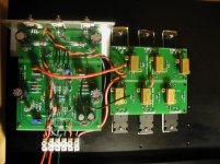
Here is a pic. the 2SA1943 is on bottom, and 2SC500 on top.
Power is fed to input and driver board from connector at bottom. . Output power is fed by input board.
I have the two NPN/PNP outputs connected (red jumper) and then meeting up with the FB (green wire) at the connector which goes to the + speaker binding post...
With this config, I connect the attenuated signal input from CD player to the input board, and speaker output from power GRND and FB/Output, and I get very high voltage (near rail voltage) at outputs...
If your front end is working like mine you will get the following voltages:
r103, r107 (rail-0.6v)
r108, r109 (rail-27v)
r112, r113, r116, r117 ~2.2v
r120, r121 ~1.59v
r122, r123 ~1v
(voltages measured across the identified resistor)
Now I cannot get the outputs resistors (via R126 bias pot) higher than .03v. The collectors of output transistors are are all seeing near rail voltage.
Here is a pic. the 2SA1943 is on bottom, and 2SC500 on top.
Power is fed to input and driver board from connector at bottom. . Output power is fed by input board.
I have the two NPN/PNP outputs connected (red jumper) and then meeting up with the FB (green wire) at the connector which goes to the + speaker binding post...
With this config, I connect the attenuated signal input from CD player to the input board, and speaker output from power GRND and FB/Output, and I get very high voltage (near rail voltage) at outputs...
Attachments
Just noticed something - the input board does not have a power ground labeled, but I connected the power ground to the leftmost GRND connection of the three listed. I will try to disconnect it to see if that is it...
The Driver board is the only board that has a POWER GROUND connection, correct? None on output boards and none on input boards?
EDIT - From what I have read, the Power GRD connections are correct...
regarding my previous pic at the connector on bottom from right to left...
Output to + speaker terminal
Signal in
Signal Ground
No Connection
Power Ground - Star Ground (both input and driver boards to metal tab at power caps)
-V Rail
+V Rail
Whoa, just noticed that both pots may be soldered on the input board backwards....
But getting correct values on the front end....what gives???
But getting correct values on the front end....what gives???
Some voltages...R649 output resistors with .04v bias fully turned up.
Voltages on Q109 BCE
2.4
40
1.7
Voltages on Q110 BCE
-1.7
-40
-1.1
Voltages on Q111 BCE
-1.1
2.3
-1.7
Voltage on Q506 2SC5200 BCE
.922
40
.314
Voltage on Q503 2SA1943 BCE
-.372
-40
.235
Voltages on Q109 BCE
2.4
40
1.7
Voltages on Q110 BCE
-1.7
-40
-1.1
Voltages on Q111 BCE
-1.1
2.3
-1.7
Voltage on Q506 2SC5200 BCE
.922
40
.314
Voltage on Q503 2SA1943 BCE
-.372
-40
.235
I haven't got a Krell I can easily take apart to check your voltages at the moment, but do you have a scope?
Unfortunately, no. A working scope I do not have...
Would a reversed installed bias and offset pot do such a thing? It seems to work correctly (lower bias CW) and all voltages across driver and input board resistors seem good as I posted.
Maybe bad OP transistors? But all bad?
Would a reversed installed bias and offset pot do such a thing? It seems to work correctly (lower bias CW) and all voltages across driver and input board resistors seem good as I posted.
Maybe bad OP transistors? But all bad?
check that the voltage Vbe of each of the transistor ~600mV and that the polarity is correct for each NPN and PNP. Your measurements show ~600mV so the first part is satisfied.
The emitter voltages of Q109/Q110 should be identical to the base voltage values of the output devices, means there's something wrong with the connection to the output stage.
Adjust the DC-setting of the front end first, the DC output voltage is off by 600mV.
Adjust the DC-setting of the front end first, the DC output voltage is off by 600mV.
The emitter voltages of Q109/Q110 should be identical to the base voltage values of the output devices, means there's something wrong with the connection to the output stage.
I realized this from a few posted voltages, but isn't there the 2.2 ohm resistor between them? I don't see how they can be the same, or am I missing something?
I have confirmed that the resistance between driver emitter to output base is 2 ohm...is this the issue??
BTW - I am measuring the above voltages with respect to power ground.
DC current gain of the A1943/C5200 is well above 100 up to several amps of emitter output current.
If you bias the output stage to 50W/8, it's 600mA for each of the 6 devices.
600mA / 100= 6mA, 6mA times 2.2 Ohms is only 13.2mV voltage loss across the base resistors.
If you bias the output stage to 50W/8, it's 600mA for each of the 6 devices.
600mA / 100= 6mA, 6mA times 2.2 Ohms is only 13.2mV voltage loss across the base resistors.
So 2.2 ohm resistor may be incorrect?
I confirm 600mv on all driver and output transistors.
With Driver resistor biased to 1.2V, I get 19mv on output emitter resistor (.649 ohm 10W)
And 625mv across output base resistor (2.2 ohm 1/4W).
I confirm 600mv on all driver and output transistors.
With Driver resistor biased to 1.2V, I get 19mv on output emitter resistor (.649 ohm 10W)
And 625mv across output base resistor (2.2 ohm 1/4W).
No, it means the 2.2 ohm resistor makes little difference.
Certainly not 700-800mV difference.
Certainly not 700-800mV difference.
Sorry, I edited my previous post after jacco's reply...
I am getting that 625mv across that 2r2 base resistor....
The 2SA1943 (PNP) are on the - drive/-V rail side of outputs, and 2SC5200 (NPN) is on the + drive/+V rail side, of output board just as the schematic shows...
That is 600mv across Base/Emitter of all driver and output transistors...
I am getting that 625mv across that 2r2 base resistor....
The 2SA1943 (PNP) are on the - drive/-V rail side of outputs, and 2SC5200 (NPN) is on the + drive/+V rail side, of output board just as the schematic shows...
I confirm 600mv on all driver and output transistors.
That is 600mv across Base/Emitter of all driver and output transistors...
Has the base resistor gone open circuit?
Temporarily add a second 2r2 in parallel to the suspect one and remeasure the Vdrop.
Temporarily add a second 2r2 in parallel to the suspect one and remeasure the Vdrop.
- Home
- Amplifiers
- Solid State
- Krell KSA 50 PCB