Yes, he mentioned he measured on C1 right from the start.
This should give me about 23.5VDC Vin across C1, but i' m actually measuring Vin about 21.2VDC.
Sure you can but don't completely avoid a C1 capacitor. It also plays the role of local decoupling for the PCB. There can be strong oscillation with the incoming wires inductance if without any local input capacitance. Put a 100uF in its place.
Thanks for your reply. I have two more questions:
1. What is the min. difference between input voltage and output voltage?
2. What is the symptom of oscillation? Voltage fluctuation at output? How can I check if the regulator is stable or not?
1. Absolutely essential are 1.7V at 200mA and 2.5V at 600mA. Lower than those and the constant current source starts losing mA from its normally programmed draw. In other words it softens its function after those points until it loses it when going further down. So for provision against mains fluctuation chances and for acceptable pF parasitic in M1 (speedier with more DCV across it) some basic 5V difference is recommended.
2. Its AC waveform produced and superimposed on the DC level. Several kHz or MHz. Can manifest as buzz noise and/or quality breakdown in the audio end of things. Best observed with an oscilloscope AC coupled in low mV vertical setting when probing the rail. This version is not particularly prone to misbehavior if you will follow its pdf guide document as attached in post#1
2. Its AC waveform produced and superimposed on the DC level. Several kHz or MHz. Can manifest as buzz noise and/or quality breakdown in the audio end of things. Best observed with an oscilloscope AC coupled in low mV vertical setting when probing the rail. This version is not particularly prone to misbehavior if you will follow its pdf guide document as attached in post#1
I haven't heard about SSLV till those days, unfortunately.Do you ever make any SSLV shunt in Kyiv by the way?
Hi salas, I was curious about the simulation and its stability and when I did the same simulation as per the first post and what I found is oscillation at any value. Infact I have got all the same models instead of substitutes. Im curious that if anything to be corrected in the schematic or is the reg stable as is? If its stable then why is it oscillating for any resistor value ( consider increasing the gate resistors ) its not getting stabilized.
Attachments
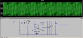
Fact is it doesn't oscillate because its in use by people and works fine. It does not oscillate in my simulation either. Its calculated for 60 degrees phase margin at 100mA spare. There is the open loop gain curve in post#1 with cross hairs at zero dB showing that. Must be some wrong models you use. The BJTs & MOSFETs I see in your schematic are different types. Don't forget to add the recommended ESR in your simulated output capacitor too.
Thank you for the reply salas so I have a question that what if top stop the oscillation in the simulation? do i need to add 100uF between the base of Q2 and ground? ( But can we do this in reality? like to reduce the oscillations if occurs ? using 100uF wouldn`t that degrade the performance of the reg?Fact is it doesn't oscillate because its in use by people and works fine. It does not oscillate in my simulation either. Its calculated for 60 degrees phase margin at 100mA spare. There is the open loop gain curve in post#1 with cross hairs at zero dB showing that. Must be some wrong models you use. The BJTs & MOSFETs I see in your schematic are different types. Don't forget to add the recommended ESR in your simulated output capacitor too.
I have used the same transistors as you have used in the simulation. May be the model source might be different. I have got the models from diyamp.txt and kt cordell models and some Jfet libs available online.
If you have a working schematic and models can you share it.
If you have a working schematic and models can you share it.
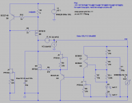
My LTspice .asc is linked to my computer's customized libraries so it will not run self standing on other computers. I give you the models I used while the 327-40s are internal LTspice ones you can call up just by picking or stating them. Don't pay attention to the designations vs the PCB schematic like which one is M1 Q1 etc. they are random here.
.model PF5102 NJF(Beta=14.28m Betatce=-.5 Rd=1 Rs=1 Lambda=8m Vto=-.9723
+ Vtotc=-2.5m Is=205.2f Isr=1.988p N=1 Nr=2 Xti=3 Alpha=20.98u
+ Vk=123.7 Cgd=10.76p M=.4069 Pb=1 Fc=.5 Cgs=9.56p Kf=493.1E-18
+ Af=1)
.model BC560C PNP(Is=1.02f Xti=3 Eg=1.11 Vaf=34.62 Bf=401.6 Ise=38.26p
+ Ne=5.635 Ikf=74.73m Nk=.512 Xtb=1.5 Br=9.011 Isc=1.517f
+ Nc=1.831 Ikr=.1469 Rc=1.151 Cjc=9.81p Mjc=.332 Vjc=.4865 Fc=.5
+ Cje=30p Mje=.3333 Vje=.5 Tr=10n Tf=524p Itf=.9847 Xtf=17.71
+ Vtf=10)
* PHILIPS pid=bc559c case=TO92
* 91-08-02 dsq
*$
.model IRF9610 PMOS(Level=3 Gamma=0 Delta=0 Eta=0 Theta=0 Kappa=0.2 Vmax=0 Xj=0
+ Tox=100n Uo=300 Phi=.6 Rs=.721 Kp=10.37u W=.64 L=2u Vto=-3.814
+ Rd=1.524 Rds=888.9K Cbd=222.3p Pb=.8 Mj=.5 Fc=.5 Cgso=1.517n
+ Cgdo=30.29p Rg=2.4 Is=886.1E-18 N=4 Tt=1100n)
* Int'l Rectifier pid=IRFC9210 case=TO220
* 88-08-25 bam creation
*$
.model IRF530 NMOS(Level=3 Gamma=0 Delta=0 Eta=0 Theta=0 Kappa=0.2 Vmax=0 Xj=0
+ Tox=100n Uo=600 Phi=.6 Rs=58.53m Kp=20.73u W=.68 L=2u Vto=3.191
+ Rd=38.69m Rds=444.4K Cbd=1.151n Pb=.8 Mj=.5 Fc=.5 Cgso=876.7p
+ Cgdo=261.4p Rg=4.63 Is=1.861p N=1 Tt=125n)
* Int'l Rectifier pid=IRFC130 case=TO220
* 88-08-25 bam creation
*$
Copy the simulation schematic, draw it to your LTspice by also adding all the voltage & current sources you see, write the exact spice black commands and values. Don't forget the ESR and ESL you see in the 33uF cap. The Vi Ii {} statements are for AC Amplitude in the small signal entry area for sources, x is a label net. Run AC analysis as written and right click on its window to add trace -1/(1-1/(2*(I(Vi)@1*V(x)@2-V(x)@1*I(Vi)@2)+V(x)@1+I(Vi)@2))
You should see the second pic's phase result at 0dB gain when with 3Ω CC resistor (200mA CC leaves 150mA shunt current after 50mA output load). This result when subtracted from -180 degrees gives the phase margin. The 25V input source has 200mV 120Hz added ripple also in case you will go looking for PSRR.
Finally, when you simply run .op (DC analysis) you will see a straight 15V green line at the output, nothing like the green fuzz in your picture.
Attachments
Does the sound quality improves over higher CCS?
Can I use longer distance wiring with sense to a distance of 1feet?
Not particularly after 200mA shunt (spare) current. Don't run sense lines, not even short ones, this version is not friendly to sense lines at all. The official board does not have such lines for a reason. I had them on the very first test board with DIP switch (there are photos in early posts) and they proved too specific for dressing and termination parts to handle, very dangerous to oscillate, talking from experience.
The high loop gain and extended bandwidth makes it specific enough for local output capacitor value & ESR range wanting it in close proximity with good tight layout. When you widen the physical loop area it upsets. This is a version with boosted drive to output and its demanding for details. Sense lines extend loop area and also add inductance. Has not to do with a remedy of changing some circuit values. Its geometrical and parasitic related disturbance to a pushed topology. You could use the 1.1 version which is much more friendly to sense than 1.2 and 1.3 if you must have it. The higher the version the more exact the implementation.
- Home
- Amplifiers
- Power Supplies
- Salas SSLV1.3 UltraBiB shunt regulator