gootee: yup re load transients. likewise nowhere has >> 1.3 metric clues.
my pet peeve: caps across rectifier diodes. FFS whats happening is that rectifier snap-off triggers a parasitic oscillation with the transformer leakage inductance and whatever stray capacitance is lurking around (rectifier, xfmr etc). slapping even more capacitance across the rectifier isnt going to help much - it'll move the resonant frequency down, but unless you happen to be pretty lucky, the resultant system is still going to be extremely poorly damped.
the solution is to place RC dampers across the diodes. or, easier, and RC damper across the rectifier AC input (hint: EXACT same result as RC damper in SLVA255).
this works, and works well. years ago I designed and built a linear regulator based on one I saw in IIRC Elektor - it had a series FET on the input, which was turned off if the L200 (Vin-Vout) got too large. needless to say this presented quite a thump to the xfmr leakage + Cstray, and an RC damper was REALLY necessary. but worked awesomely well.
its dead easy to do, too, with almost no maths:
1. measure Tring = 2pi*sqrt(Ls*Cs)
2. add some C, until Tring2 = 2pi*sqrt(Ls*(Cs+Cadd)) doubles
3. then Cadd = 3*Cs, so Cs = Cadd/3
4. then calculate Ls = (1/Cs)*(Tring/2pi)^2
5. then calculate Zo = sqrt(Ls/Cs)
6. use Rdamp = Zo, Cdamp = Cadd = 3*Cs
7. measure the result and be happy (or, twiddle Rs a but and see if you can do better)
If you can use a calculator, then adding any Cadd will suffice - just make sure that Tring2 is a fair bit bigger than Tring (we are looking really at the change in Tring, if they are very close then this is very small, so measurement SNR = bad). in practice I have found a 50% change in Tring to be more than enough - and I've done this from Hz to GHz (just).
Erickson/Maksimovic have a great writeup of this in their "fundamentals of power electronics" book (2nd ed. chapter 10 - input filter design). for the pedantically inclined, as Cadd -> infinity, Rdamp -> Zo; depending on the precise form of the damping, there is a relationship between n = Cdamp/Cs, Zo and the optimal damping resistor Rdamp. but for realistic Cadd, this doesnt amount to a big change, and is easy to measure & fiddle on the bench, with Rdamp = Zo being a very, very good initial guess.
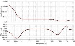
Wow. That's a really-good output impedance plot.
Please let us know some results from your breadboard version.
Hi Gotee,
thanks. I'm ordering parts, then I'll let you know practical results.
BTW, it seems too good to be true, I believe I'll have to make some tuning.
Andrea
gootee: yup re load transients. likewise nowhere has >> 1.3 metric clues.
my pet peeve: caps across rectifier diodes. FFS whats happening is that rectifier snap-off triggers a parasitic oscillation with the transformer leakage inductance and whatever stray capacitance is lurking around (rectifier, xfmr etc). slapping even more capacitance across the rectifier isnt going to help much - it'll move the resonant frequency down, but unless you happen to be pretty lucky, the resultant system is still going to be extremely poorly damped.
the solution is to place RC dampers across the diodes. or, easier, and RC damper across the rectifier AC input (hint: EXACT same result as RC damper in SLVA255).
this works, and works well. years ago I designed and built a linear regulator based on one I saw in IIRC Elektor - it had a series FET on the input, which was turned off if the L200 (Vin-Vout) got too large. needless to say this presented quite a thump to the xfmr leakage + Cstray, and an RC damper was REALLY necessary. but worked awesomely well.
its dead easy to do, too, with almost no maths:
1. measure Tring = 2pi*sqrt(Ls*Cs)
2. add some C, until Tring2 = 2pi*sqrt(Ls*(Cs+Cadd)) doubles
3. then Cadd = 3*Cs, so Cs = Cadd/3
4. then calculate Ls = (1/Cs)*(Tring/2pi)^2
5. then calculate Zo = sqrt(Ls/Cs)
6. use Rdamp = Zo, Cdamp = Cadd = 3*Cs
7. measure the result and be happy (or, twiddle Rs a but and see if you can do better)
If you can use a calculator, then adding any Cadd will suffice - just make sure that Tring2 is a fair bit bigger than Tring (we are looking really at the change in Tring, if they are very close then this is very small, so measurement SNR = bad). in practice I have found a 50% change in Tring to be more than enough - and I've done this from Hz to GHz (just).
Erickson/Maksimovic have a great writeup of this in their "fundamentals of power electronics" book (2nd ed. chapter 10 - input filter design). for the pedantically inclined, as Cadd -> infinity, Rdamp -> Zo; depending on the precise form of the damping, there is a relationship between n = Cdamp/Cs, Zo and the optimal damping resistor Rdamp. but for realistic Cadd, this doesnt amount to a big change, and is easy to measure & fiddle on the bench, with Rdamp = Zo being a very, very good initial guess.
Terry,
Wow, that's one of MY pet peeves, too! I have posted what amounts to the same procedure, at http://www.diyaudio.com/forums/powe...lm-caps-electrolytic-caps-30.html#post2828689 . Thanks for the additional details! (The only difference is that I read somewhere that Cdamp should be 4xCs to 10xCs, so that's what I posted.)
And as you can see at http://www.diyaudio.com/forums/digi...ordinary-diodes-vs-schotky-4.html#post3104879 , I was beating the same drum, again, only three days ago.
And just yesterday I was trying to set up a simple LT-Spice simulation of a linear PSU, with component and conductor parasitics, but also with a more-realistic-than-usual model of an AC power transformer, to demonstrate reservoir and decoupling cap issues, and had a heck of a time getting the damping good-enough. There were three different modes, with one needing something over 7k of R (which needed no Cdamp, of course). I think I had a huge ringing at 436 kHz, and some 26.4 MHz, and then also some 74.9 kHz. And there are still some remnants of the 26.4 MHz that I couldn't eliminate, maybe because the snubber component values are interacting a little, some being in parallel. Now I'm thinking that I need to revisit the transformer model, instead of going to all this trouble.
Cheers,
Tom
Hi Gotee,
thanks. I'm ordering parts, then I'll let you know practical results.
BTW, it seems too good to be true, I believe I'll have to make some tuning.
Andrea
Andrea,
It will be very interesting to find out how good it can be, in hardware.
Maybe you should add the parasitics of the CONDUCTORS to your simulations, now, so you can possibly determine the sensitivity to them, and if needed, which conductors need to be the shortest, etc, which might be critical to the implementation layout design.
I usually at least put an inductor in each conductor, in LT-Spice, which allows entry of a series resistance in the inductor properties, enabling inclusion of both parasitic inductance and parasitic resistance with the use of only one component.
I parameterize both the inductance and series resistance of each parasitic inductor, in terms of the length of the conductor, making the length a variable that I can set on the schematic, for each conductor.
For a typical rule-of-thumb estimate, the inductance is then entered as {len*25n} and its series resistance is then {len*1m}, if len is in inches. Or, equivalently, you could use 1nH per mm and .00003937 Ohms per millimeter, or change that to whatever length units you prefer. For better numbers, there are pcb trace impedance calculators, on line.
Actually, I also make the nH and Ohms per unit length into variables, just in case.
Anyway, then it would be easy to step the length of any conductor through a range of values, with ".step param len start end increment", where you supply the start, end, and increment values, and your "len" variable's name (or you can use the "list" format of the .step command). Then, LT-Spice automatically runs all of the simulations (for the steps) without stopping, and at the end it plots all of the curves on one plot. It's very handy, sometimes!
You can even do TWO step commands at once, which makes it do the second one's entire sequence of steps for each step in the first one, and then it plots ALL of them on one plot. (But don't worry, you can turn on or off any range of steps, while viewing the plot.)
Cheers,
Tom
Last edited:
Hi Gotee,
thanks. I'm ordering parts, then I'll let you know practical results.
BTW, it seems too good to be true, I believe I'll have to make some tuning.
Andrea
Andrea,
The impedance of the conductors from the output to the load could easily be significant.
If a multilayer PCB with "real" power and ground planes will not be used, then the following might be relevant.
If you cannot locate the output right at the load, then you might want to consider using multiple parallel conductors, in place of each single conductor from the output to the load.
You could then make the inductance and resistance of the conductors as low as you want them to be, by using a large-enough number of them in parallel.
It does work. And you can simulate it as well. If you simulate the conductos to the load, then you will also be able to determine the impedance as seen by the load, which is the only place where it is important, and you could then also determine any necessary decoupling capacitor values, and the inductance and resistance that could be tolerated in their connections to the load. Sometimes, then, you might find that multiple parallel caps are needed (in order to get the total decoupling impedance low-enough), with no mutual inductance in their connections to the load (so the inductance reduces fully due to paralleling). In that case, if parallel conductors are already being used, implementing the decoupling capacitor layout should be easier.
Cheers,
Tom
That's certainly a good part of the story, Tom. If one introduces every realistic parasitic element all of a sudden those nice clean waveforms of the textbooks degenerate into a bit of a nasty bundle of transitory high frequency artifacts, which in turn vary depending on precisely what the current draw is at the moment. I love the SPICE models of a circuit being fed pristine pure DC voltages, everyone can have fantasies after all ...have you ever tried listening to a misbehaving power supply?And just yesterday I was trying to set up a simple LT-Spice simulation of a linear PSU, with component and conductor parasitics, but also with a more-realistic-than-usual model of an AC power transformer, to demonstrate reservoir and decoupling cap issues, and had a heck of a time getting the damping good-enough. There were three different modes, with one needing something over 7k of R (which needed no Cdamp, of course). I think I had a huge ringing at 436 kHz, and some 26.4 MHz, and then also some 74.9 kHz. And there are still some remnants of the 26.4 MHz that I couldn't eliminate, maybe because the snubber component values are interacting a little, some being in parallel. Now I'm thinking that I need to revisit the transformer model, instead of going to all this trouble.
Cheers,
Tom
Reality trumps every time ...
Frank
Tom,
for optimal damping an LC network with an R-C network in parallel with the C, the detailed solution is:
n = Cdamp/Cring, Zring = sqrt(Lring/Cring)
peak L-C network output impedance is: |Zout| = Zring*sqrt(2*(2+n)/n
this occurs at Fpeak = Fring*sqrt[2/(2+n)]
Optimum Q = Rdamp/Zring = sqrt[(2+n)*(4+3n)]/sqrt[(2n^2)*(4+n)]
(I put sqrts on num & dem to save elleventy brackets)
a reasonable approximation is Qopt = 1.5*n^(-0.7), n < 10
a much better approximation is Qopt = 1.09*n^(-0.97) + 0.35, n < 10
then the optimum damping resistor is Rdamp = Qopt*Zring
so once you've determined Lring and Cring, you choose the Cdamp you're happy with (size, cost and AC line/harmonic currents all limit how large a Cdamp you can have).
this then gives n, and you can simply calculate Rdamp = Zring*1.5*n^(-0.7)
for n = 3 we get:
Qopt_exact = 0.718
Qopt_approx = 0.695 (-3.2%)
Qopt_approx2 = 0.726 (+1.1%)
so Rdamp = 0.72*Zring when Cdamp = 3*Cring
or, if you're happy with Q = 1 then Rdamp = Zring and n = 1.729
(and you can see why 2...3xCring is a reasonable compromise)
if you're damping parasitic oscillations, Cring is pretty small and there aren't many constraints on size or value (they'll all be in the same package). but larger Cdamp causes more losses in Rdamp due to the non-ringy (eg AC line or Fsmps) voltage swing. for AC line frequencies I've happily used n > 10, otherwise I tend to pick 2 < n < 4 for convenient Cring
when damping LC filters its usually a physical size and/or value constraint, and I aim for 1 < n < 2 (unless I really, really need to keep Zdamped low)
Tom,
for optimal damping an LC network with an R-C network in parallel with the C, the detailed solution is:
n = Cdamp/Cring, Zring = sqrt(Lring/Cring)
peak L-C network output impedance is: |Zout| = Zring*sqrt(2*(2+n)/n
this occurs at Fpeak = Fring*sqrt[2/(2+n)]
Optimum Q = Rdamp/Zring = sqrt[(2+n)*(4+3n)]/sqrt[(2n^2)*(4+n)]
(I put sqrts on num & dem to save elleventy brackets)
a reasonable approximation is Qopt = 1.5*n^(-0.7), n < 10
a much better approximation is Qopt = 1.09*n^(-0.97) + 0.35, n < 10
then the optimum damping resistor is Rdamp = Qopt*Zring
so once you've determined Lring and Cring, you choose the Cdamp you're happy with (size, cost and AC line/harmonic currents all limit how large a Cdamp you can have).
this then gives n, and you can simply calculate Rdamp = Zring*1.5*n^(-0.7)
for n = 3 we get:
Qopt_exact = 0.718
Qopt_approx = 0.695 (-3.2%)
Qopt_approx2 = 0.726 (+1.1%)
so Rdamp = 0.72*Zring when Cdamp = 3*Cring
or, if you're happy with Q = 1 then Rdamp = Zring and n = 1.729
(and you can see why 2...3xCring is a reasonable compromise)
if you're damping parasitic oscillations, Cring is pretty small and there aren't many constraints on size or value (they'll all be in the same package). but larger Cdamp causes more losses in Rdamp due to the non-ringy (eg AC line or Fsmps) voltage swing. for AC line frequencies I've happily used n > 10, otherwise I tend to pick 2 < n < 4 for convenient Cring
when damping LC filters its usually a physical size and/or value constraint, and I aim for 1 < n < 2 (unless I really, really need to keep Zdamped low)
Beautiful!!
Thanks!!!
Oh, I forgot to add:
being very lazy I couldn't be bothered figuring out the relevant formulae. So I'd measure L&C as described, choose Cdamp then do a spice simulation sweeping Rdamp from Zring/10 to 10*Zring to pick the optimum value.
Then I got a copy of Erickson & Maksimovic, and they'd helpfully worked it out for me.
Oh, I forgot to add:
being very lazy I couldn't be bothered figuring out the relevant formulae. So I'd measure L&C as described, choose Cdamp then do a spice simulation sweeping Rdamp from Zring/10 to 10*Zring to pick the optimum value.
Then I got a copy of Erickson & Maksimovic, and they'd helpfully worked it out for me.
Sounds perfect, to me. I've probably done more than my share of step sweeps in LT-Spice, for similar reasons. I wish it had an optimizer built-in, kind of like the one in the 4NEC2 antenna-simulation software (but much better). Thirty years ago, I never bothered memorizing any equations. Back then I could just rederive them on the spot. But rust never sleeps.
I'm going to go look for that book right now, on Amazon. I've been buying a lot of books, lately, mostly technical, and CDs too, mostly musical.
Cheers,
Tom
Edit: Ordered it. New hardcover 2nd edition for $70 + $3.99 shipping. Wow, I saw Grover's "Inductance Calculations" for only $10, on Amazon. (I already have a nice new hardcover of it.)
Last edited:
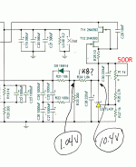
Are these values correct? -- as the voltage divider after the reference U3 knocks the voltage down by 90%.
Yes. values are correct. The voltage coming from the TL431 is divided by 10 to reduce the noise of the voltage reference, then there is a LPF with a very low corner frequency to reduce noise again.
Finally the voltage of the reference is about 1V, with a very low noise.
The TL431 is not just a low noise voltage reference, so I used these tecniques to reduce drastically its noise.
Andrea
Seems like a lot of work to derive the reference voltage is my point -- you could use an LM4041-1.2 which is a $0.334 part. Even a button cell would be less expensive, low noise, take up less space and last several years!
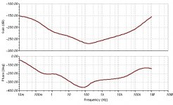
By the way, the standard TL431 model (from TI) doesn't contain the reactive elements. When I simulate the circuit I get a smoothly rising Z-curve, but it's not flat.
You might want to take the curve out to 20MHz and see the effect of not connecting the compensation pin on the AD797,
By the way, the standard TL431 model (from TI) doesn't contain the reactive elements. When I simulate the circuit I get a smoothly rising Z-curve, but it's not flat.
You might want to take the curve out to 20MHz and see the effect of not connecting the compensation pin on the AD797,
Seems like a lot of work to derive the reference voltage is my point -- you could use an LM4041-1.2 which is a $0.334 part. Even a button cell would be less expensive, low noise, take up less space and last several years!
By the way, the standard TL431 model (from TI) doesn't contain the reactive elements. When I simulate the circuit I get a smoothly rising Z-curve, but it's not flat.
You might want to take the curve out to 20MHz and see the effect of not connecting the compensation pin on the AD797,
In my simulation, adding the ESR and ESL of the output caps (Panasonic FC 3 x 390 uF / 35V 0.12 tan/d), Z rises smoothly with a peak of 2.2 mOhm around 1 MHz, then decreases again around 1.3 mOhm and remain flat up to 10G, without phase shift.
No effect removing the compensation of AD797 and probably it could be oscillate.
I think the rising of the output impedance comes from the high feedback loop around the AD797, and the output caps should act the right compensation.
BTW, I have ordered all parts to prototype the circuit to see how it will really perform. Surely it will need some adjustements.
How would a CCS fed, LED compare?.............The voltage coming from the TL431 is divided by 10 to reduce the noise of the voltage reference, then there is a LPF with a very low corner frequency to reduce noise again.
Finally the voltage of the reference is about 1V, with a very low noise.
The TL431 is not just a low noise voltage reference, so I used these tecniques to reduce drastically its noise.....
How would a CCS fed, LED compare?
With a CCS the voltage reference see an higher impedance.
About the LED... I prefer the voltage reference, since the TL431 is cheap, I use it also in the preregulation stage as the feedback error amplifier, it has an adjustment pin suitable for fine voltage setting with low current flowing in the trimmer resistor, less drift.
Are you sure that schematic is right? The common mode input range of the AD797 is about +-3 to 3.5V with a +-6V supply or 6+- 3 to 3.5V with a 12V supply. I don’t think you will be able to compare voltages that close to ground with that op-amp.
You're right, in fact I measured 1.34V at non inverting input of the op amp because some current flows through op amp input to LPF.
I have changed the network divider to set voltage reference to 2.5V and so seems to work properly.
Attachments
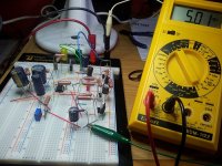
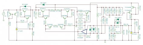
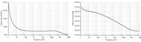
The breadboard seems to confirm the simulation: very stable, no oscillation, noise under the noise floor of my equipment.
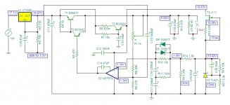
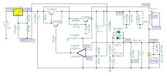
Follows the breadboard final schematic and simulations already posted.
Before making a PCB prototype I simulated some popular regulators, follows my results, with parasitics ESL and ESR of used capacitors.
Follows the breadboard final schematic and simulations already posted.
Before making a PCB prototype I simulated some popular regulators, follows my results, with parasitics ESL and ESR of used capacitors.
Attachments
- Home
- Amplifiers
- Power Supplies
- The Well Regulated Power Supply