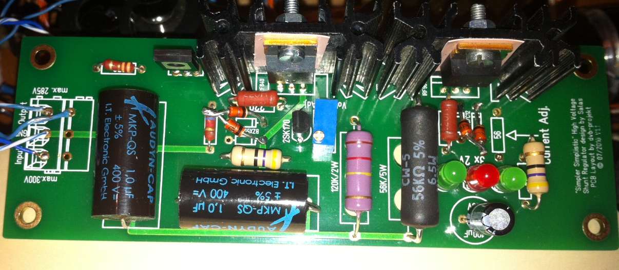
Could it be that the heatsink shown has Rth s-a=5C/W. That's what my manufacturer tells me. I only had one, I needed two.Also, Q3 (IRF840) was running very hot, 125C on the heatsink. The heatsink used is attached (2.6C/W) DK part HS380-ND. That heat seemed way...too much for reasons unknown.
Heat indeed. 4k7 should help. Do you have any TO-92 mini sink to put on Q2 also? How much dissipation it shows on your sim for 4k7? If you now run 50mA excess X 250Vo = 12.5W steady...If you set 35mACCS-10mA to load=25mA excess it will be 6.25W, big relief for the IRF840 on that smallish sink. Yes the newer one with the simpler Jfet Norton Vref I find better in general. But listen to the one you got first so to do your own comparisons later with the newer.
Dear Salas,
I have done some adjustments in the model so I can better understand what is happening. First, the current (from LT Spice simulation) I will need for the circuit (2x 6DJ8) in Class A is about 15mA maximum. So for 250V plate supply, this load resistor will be about 17K for the regulator simulation. I'm also using a HV heater divider reference circuit on the regulator's output to insure the cathode to heater maximum isn't exceeded. This uses just 1.2mA. So the total current will be about 16mA.
So here's where I'm a little confused: when you specify the current needs to be double, is this double what the actual load current is, or do I need to include what is consumed in the circuit? For example, on the circuit section (leg) with R5, this is about 4mA current. Or does the factor of *2 include compensation for currents consumed by the circuit itself?
One other question please - which post shows the details on the correct way to calculate for the CCS? This is still a bit unclear.
With these changes, the simulation shows a power dissipation of just 2.7W across the IRF840 - this does not explain the extreme heatsink temperatures of 125C.
With the change to resistor R4 to 4.7K, the power dissipation of Q2 has now become 280mW, which should be sustainable. I might have a clip-on heatsink, if not I will get one.
Now, I am very curious about the newer design. What differences might be heard, and also importantly - is this design more stable and reliable? This is quite important to me in addition to sound.
Best regards,
Gary
Could it be that the heatsink shown has Rth s-a=5C/W. That's what my manufacturer tells me. I only had one, I needed two.
Hi,
Which specification are you referring to? The junction to ambient? Here's the specifications on that heatsink:
Power Dissipation @ Temperature Rise 20W @ 60°C
Thermal Resistance @ Forced Air Flow 2.0°C/W @ 300 LFM
Thermal Resistance @ Natural 2.6°C/W
So for the Pd I am dissipating, it should be ok...something weird going on, I'm sure.
Gary
Dear Salas,
I have done some adjustments in the model so I can better understand what is happening. First, the current (from LT Spice simulation) I will need for the circuit (2x 6DJ8) in Class A is about 15mA maximum. So for 250V plate supply, this load resistor will be about 17K for the regulator simulation. I'm also using a HV heater divider reference circuit on the regulator's output to insure the cathode to heater maximum isn't exceeded. This uses just 1.2mA. So the total current will be about 16mA.
So here's where I'm a little confused: when you specify the current needs to be double, is this double what the actual load current is, or do I need to include what is consumed in the circuit? For example, on the circuit section (leg) with R5, this is about 4mA current. Or does the factor of *2 include compensation for currents consumed by the circuit itself?
One other question please - which post shows the details on the correct way to calculate for the CCS? This is still a bit unclear.
With these changes, the simulation shows a power dissipation of just 2.7W across the IRF840 - this does not explain the extreme heatsink temperatures of 125C.
With the change to resistor R4 to 4.7K, the power dissipation of Q2 has now become 280mW, which should be sustainable. I might have a clip-on heatsink, if not I will get one.
Now, I am very curious about the newer design. What differences might be heard, and also importantly - is this design more stable and reliable? This is quite important to me in addition to sound.
Best regards,
Gary
Hi, the minimum is to allow +25mA on top of your load's consumption. That will take care of the internal needs of the reg and will keep its Zo to spec. If you have enough sinking, double the load's consumption + 25mA will give even better damping.
The CCS runs on Iccs=(3xLed'sVdrop-Vgs)/R1. So there is some slack for tolerances of Vgs and Vf of chosen Leds for each builder. When you will measure the drop across your now R1 you will know what R1 value to use for your target Iccs.
I suspect you run more current than the simulator thinks with the Vgs and Leds it sims. Measure it. Your 840 probably consumes more excess than calculated. 125C is still too much, maybe its oscillating also. Do you have a picture so I can see the layout? Give the 6520 a 47R base stopper, use lower, 220R gate stoppers on the Mosfets.
280mW seems cool.
The older one will give warmer bass, more classic tone. The upper BC transistor Q4 provides Vbe ref for the trimmer to Isource, the lower one Q5 buffers it to the Norton Vref created by I to V on the ref resistor. If you will decouple the base resistor R8 to ground with a 47uF/350V you will get more slam. The newer one has one less tempco, relies on Idss not Vbe, no Ib currents to settle. Has the slam without the extra lytic cap. Has a more modern tone. Some may prefer the older mind you, depends on synergy with the rest. Both have been running for long, the newer has many more happy campers due to some GBs and PCBs made, so its statistically more proven.
I hope that I covered your questions.
Salas -
That sure did. I appreciate your feedback and will review what I have done based on your input.
As you are such a great teacher for all that come to this forum for what they love to do, I leave you with this quote:
"A teacher affects eternity; he can never tell where his influence stops." ~Henry Brooks Adams
Thanks for all that you do for everyone on this forum!
")
Gary
Hi, the minimum is to allow +25mA on top of your load's consumption. That will take care of the internal needs of the reg and will keep its Zo to spec. If you have enough sinking, double the load's consumption + 25mA will give even better damping.
The CCS runs on Iccs=(3xLed'sVdrop-Vgs)/R1. So there is some slack for tolerances of Vgs and Vf of chosen Leds for each builder. When you will measure the drop across your now R1 you will know what R1 value to use for your target Iccs.
I suspect you run more current than the simulator thinks with the Vgs and Leds it sims. Measure it. Your 840 probably consumes more excess than calculated. 125C is still too much, maybe its oscillating also. Do you have a picture so I can see the layout? Give the 6520 a 47R base stopper, use lower, 220R gate stoppers on the Mosfets.
Salas -
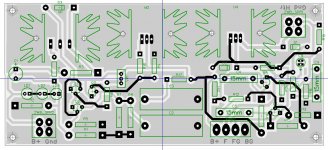
Here is the PCB layout from Diptrace. Power enters at lower left. At upper right is the unregulated DC for the filaments. At lower right is output for B+ & GND, and (HV referenced) Filament & GND.
One potential issue might be the distance of the clamping zener (D3) from the IRFP9240 - perhaps it needs to be closer?
You indicated changing the gate stoppers to 220 ohms - meaning R7 and R2?
Thank you,
Gary
280mW seems cool.
The older one will give warmer bass, more classic tone. The upper BC transistor Q4 provides Vbe ref for the trimmer to Isource, the lower one Q5 buffers it to the Norton Vref created by I to V on the ref resistor. If you will decouple the base resistor R8 to ground with a 47uF/350V you will get more slam. The newer one has one less tempco, relies on Idss not Vbe, no Ib currents to settle. Has the slam without the extra lytic cap. Has a more modern tone. Some may prefer the older mind you, depends on synergy with the rest. Both have been running for long, the newer has many more happy campers due to some GBs and PCBs made, so its statistically more proven.
I hope that I covered your questions.
Attachments
Hi Salas,
Tried the SSSSR (Salas Simpler Simplistic Shunt Regs) and they are something else. Still have to listen to them in my main system. But first impressions are favourable...very favourable.
But I just want to see if I understand this correctly. At first I dialed in the "out" voltage a little lower than the "in" voltage. And then measured the current through the current set resistor. And all I measured was the draw of the circuit plus a little more. But as I turned the pot to get a lower "out" voltage. The current went up.
Here is the question. The current set resistor (R1) only actually determines the max output current? Since the shunt current is very much dependant on the little pot...I am correct in saying that?
The Mosfets change their Vgs a little with different voltages and currents. Because the CCS current is determined by R1/(LEDS-VGS) its normal there will be a range. That is why you can see a current range given in the first posts schematics along the voltage output range. For the Simpler Simplistic keep a Vin-Vout >= 15V. Keep a CCS current (VdropR1/R1) >=25mA than your top load demand. On what audio circuit application did you try them?
Hi Salas,
On my DAC output stage.
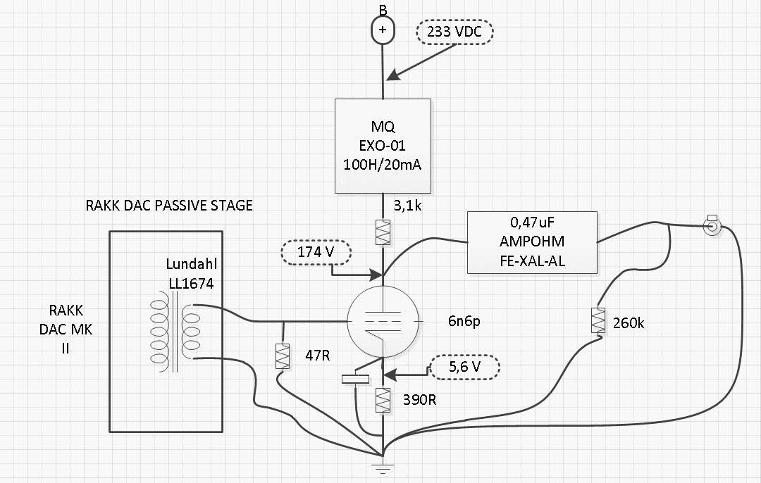
If I do Vin-Vout >= 15V there is hardly any extra shunt current at all. BUT I can already hear an improvement.
Only after Vin-Vout >= 90V there is about 55mA total current drawn. Resistor is 29R and voltage across it 1.63 or so.
I use dvb-projekt's boards.
On my DAC output stage.
If I do Vin-Vout >= 15V there is hardly any extra shunt current at all. BUT I can already hear an improvement.
Only after Vin-Vout >= 90V there is about 55mA total current drawn. Resistor is 29R and voltage across it 1.63 or so.
I use dvb-projekt's boards.
Attachments

Last edited:
I'm using one at the moment. So I was aiming for (14,5+14,5)*2+25mA=85mA.f you are using double mono regs see to have 40mA on each R1.
If you use 56R current Adj. it will set circa 40mA with average LEDS and Vgs. That is not enough if you supply two channels. The reg needs +25mA on top of that 30mA to the channels, for its own consumption purposes. 85mA is nice, drops its impedance a bit more, but your sinks look like are going to be taxed a bit. What is the value of your current Adj. resistor and what is the vdrop across it?
29R.(Two 56R in parallel) Voltage drop 1,63. And common reg for both channels yes. (But then the IRF840 and MJE350 become 90 degrees celcius) and there is major voltage drop.current Adj. resistor and what is the vdrop across it? Common reg for both channels?
Last edited:
That means 56mA CCS. Which is +26mA above your load demand. That is correct use. It also means around 6W dissipation for the IRF840 on that little sink. Maybe you have a mini sink to bolt on the MJE350? That would help it. Where and how much there is major voltage drop?
What I was trying to say is that I only get that much current to be shunted if I dial the pot way down to 135V or so. (voltage drop)Where and how much there is major voltage drop?
And I did not solder the heat sinks in because I thought they would be too small. But that is all I had that fitted. I guess I'll have to go dual mono. And I might increase the b+ by going solid state rectifier and removing the CLCLCR with just some CR.
That board was made by DVB for a certain DAC output stage, I think for under 200V B+ and less consumption. Its better you will use double mono so to have less heat when you go above 200V and the sinks to suffice. I recommend using a dummy load calculated for target load consumption at projected B+. Like 15K//15K (10W each) across 233V for 30mA, or just one for 15mA and be setting R1 for the proper +25mA margin by experiment. Then connecting to the real preamp.
- Home
- Amplifiers
- Power Supplies
- Simplistic MosFET HV Shunt Regs