Muchos gratias Felipe.
De rien Jean Charles.

So I removed my Salas SSHV board to do a listening comparison.
It seems I've lost and gained things.
What I do not like and miss without it:
-The soundstage lacks a bit of order of the placement of instruments.
-Some sounds lack a bit of punch and authority.
What I like without it:
-The sound was fatiguing and nervous with it, now it's no more.
-I gained a bit of transparency
I'd really like somehow to combine the pros without the cons. I don't enjoy the nervous sound, but I miss the authority and the soundstage the Salas gives me.")
A little bit of info about my amplifier:
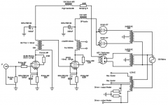
-Choke input power supply with a 6-sections high bandwidth custom choke wound by me -> Rifa PEH169 capitor -> Salas SSHV board -> 6k Interstage transformer driving 6P45S.
It seems I've lost and gained things.
What I do not like and miss without it:
-The soundstage lacks a bit of order of the placement of instruments.
-Some sounds lack a bit of punch and authority.
What I like without it:
-The sound was fatiguing and nervous with it, now it's no more.
-I gained a bit of transparency
I'd really like somehow to combine the pros without the cons. I don't enjoy the nervous sound, but I miss the authority and the soundstage the Salas gives me.
A little bit of info about my amplifier:
-Choke input power supply with a 6-sections high bandwidth custom choke wound by me -> Rifa PEH169 capitor -> Salas SSHV board -> 6k Interstage transformer driving 6P45S.
Last edited:
Maybe nervous sound means some transient oscillation. Not a typical sound experienced with SSHV. Interstage transformer inductance could be pushing the correct sense lines readings. Try it in two wire output mode. Short S0 with F0 and S+ with F+ using small links right at the output connector of SSHV. Use a thick enough twisted pair from connector to load and listen again. Keep shortest wiring distance possible between reg and load. Any + and 0 labeled output means the same at the connector now. Its normal + and ground. The sense circuit loop is closed locally at the reg by the links.
Maybe nervous sound means some transient oscillation. Not a typical sound experienced with SSHV. Interstage transformer inductance could be pushing the correct sense lines readings. Try it in two wire output mode. Short S0 with F0 and S+ with F+ using small links right at the output connector of SSHV.
This was the way it was, when I built it. Although I did lack the twisted pair. The wires from the load to the reg are the transformer's bobbin wires themselves with a length of 20cm each. I could twist them a bit.
Too low output impedance isn't critical for this application. If I could sacrifice it a bit, in order to tame this nervousity, I would be glad. For example, by putting a damping resistor in series?
I just run it. The L component did not change the open loop analysis because the DCR is enough and isolates. Maybe some more series damping for taming the peak as you say. Also make sure that the peak 2 peak load current swing does not meet the current limit of the CCS in the reg and there is at least 20mA margin. Bad limit could produce distortion. There is IXYS stronger bit slower part to use than DN2540 Q1 Q2 if limited.
Hi Salas,See first that the transistors measure Vbe like 0.6V and that the MOSFETS measure VGS like 2-4V. If not they should need replacement. If no success check with a DMM that can light up an LED on diode mode that each led is still OK as it is soldered on. Or with a battery, but be quick. Also on Ohms mode that no JFET is below 30 Ohm across D & S pins. For more discussion if not debugged easily, we can continue in the Simplistic Mosfet HV Shunt Regs thread in power supplies forum. Ready a couple of pictures we maybe can see something wrong on them if we need go there. Good luck.
So far i have removed, tested, and confirmed Q4 is ok, as is the LED. Q5 and Q6 are both toast.
With Q1 and Q2 in circuit i measure 14.2ohms across D to S so it looks like i need to remove them to test for sure. I guess i should also remove and test Q3 and the diodes too to be on the safe side.
I still have no idea why both boards failed, only thing i changed between the mock up phase, and final build was to replace the two Q3 IRF840's as i needed a bit more lead length for the final mounting. Items i used were IRF840PBF Vishay Semiconductors | Mouser
Assuming those were the correct items, does this failure mode indicate any specific issue to you as i really need to figure out what i did wrong?
Thanks again,
Mark
I can't be sure guessing, maybe some static discharge? Or some wrong wiring of the sense cables to the force cables at the load? Try two wire only connection next time in fear of an oscillation came to be? Two wire mode is simple, you just jumper S+ to F+ and S0 to F0 right at the output connector and use only the force thicker gauge for a twisted wire normal + 0 feed to the load.
Q1 and Q2 don't remove, use low voltage source on input connector say 15V with the two force cables connected together at the output. No sense wires nowhere. Then the constant current source is safely testable both for TP current setting and Q1 & Q2 VGS about 2V.
Q1 and Q2 don't remove, use low voltage source on input connector say 15V with the two force cables connected together at the output. No sense wires nowhere. Then the constant current source is safely testable both for TP current setting and Q1 & Q2 VGS about 2V.
Since i have one spare kit to pick parts from i replaced Q5/Q6, connected the two force connections, and disconnected the two sense connections and fed it 15v.
The current adjustment seems to be working fine 331mv across test point, and its pulling 33ma from my bench supply. VGS for Q1/Q2 (i assume i measure across the two outer pins?) is 1.13v. Adjustment pot also works as expected so it looks like the first section is good to go.
I've always run the boards with the sense to force connections jumpered together and just ran two wires to the constant current boards. Nothing there has changed since the mock up build.
So what happened it most probably happened in the (parallel) voltage section. Where you changed those Q3 MOSFETS for longer legs. Double check the Q3 insulation to its sink. Use a gate protection Zener even. Can be soldered underside directly at the pins. Hopping that it will blow instead of Q3 if there is a gate overdrive instability condition when on the actual load. Up the gate resistor's value even.
You would replace Q5/Q6 since gone anyway but in this arrangement only the CCS part tests out. Adjust to max mA with 15V and see does the VGS go higher also? There should be stopping at 100-110mA for adjustment. If all responds then it can't be any problem in the input section.
What does the actual preamp showing it as load? Active current sources? What kind? Is there some little capacitor across their input? That could reduce phase margin. Is there any resistive damping?
So what happened it most probably happened in the (parallel) voltage section. Where you changed those Q3 MOSFETS for longer legs. Double check the Q3 insulation to its sink. Use a gate protection Zener even. Can be soldered underside directly at the pins. Hopping that it will blow instead of Q3 if there is a gate overdrive instability condition when on the actual load. Up the gate resistor's value even.
You would replace Q5/Q6 since gone anyway but in this arrangement only the CCS part tests out. Adjust to max mA with 15V and see does the VGS go higher also? There should be stopping at 100-110mA for adjustment. If all responds then it can't be any problem in the input section.
What does the actual preamp showing it as load? Active current sources? What kind? Is there some little capacitor across their input? That could reduce phase margin. Is there any resistive damping?
Can you give me a bit more info about the zener for Q3, which type, which pins etc. I know a lot less about this solid state stuff than you seem to think i do
Max current adjustment tops out at 73ma, across Q1 i measure .973v, and Q2 measures .768v.
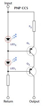
Current source boards are the same as attached pic setup for ~17ma, shunt reg boards were adjusted to 40ma.
Attachments
Last edited:
Any up to 15V Zener with cathode to gate and anode to source of Q3. Its purpose to clamp possible transient that can pierce the fine oxide layer that insulates the gate.
Try 25V test input also from the lab PSU to see if it can give some more max current. So we know more about it and to can compare other Q1 Q2 samples.
Try 10R 100uF RC locally at + input of those BJT cascode CCSs just to buffer and dampen the reg and cables form those in case something reactionary goes on at some high frequency between active circuits. There is no concern for added output resistance, only a very small voltage drop. Because a CCS is already a great series impedance towards the load.
Return CCS pin goes to some circuit point that does not impose HV across the LEDS branch or their resistor is really high?
Any up to 15V Zener with cathode to gate and anode to source of Q3. Its purpose to clamp possible transient that can pierce the fine oxide layer that insulates the gate.
Try 25V test input also from the lab PSU to see if it can give some more max current. So we know more about it and to can compare other Q1 Q2 samples.
Try 10R 100uF RC locally at + input of those BJT cascode CCSs just to buffer and dampen the reg and cables form those in case something reactionary goes on at some high frequency between active circuits. There is no concern for added output resistance, only a very small voltage drop. Because a CCS is already a great series impedance towards the load.
Return CCS pin goes to some circuit point that does not impose HV across the LEDS branch or their resistor is really high?
@25v i am still getting 75ma. That is with R4 at the end of its adjustment, 115mv-753mv across TP at each end of R4s adjustment.
Looking at the schematic, i assume D1 and D2 serve the same purpose for Q1 and Q2? I think the parts in the kit were 1N5242B so i'll add a bunch to my Mouser order. I also found the DN2540N5-G so i might as well order half a dozen of those and replace them while i am at it.
The CCS diode string has a 100k resistor as i was aiming for ~200volts into it, so only a couple of ma across the diodes to light them.
Was that 10r/100uf a typo, or did you mean 100nf?
I usually get 100-115mA with those types in that arrangement and its resistor values.
Maybe restricted VGS of Q1 which also forms the VDS for Q2 due to low IDSS DMOS sample(s). Remove D1-D2 to see if those Zeners are damaged and something changes (not that likely). You can even use 0.5W-1A diodes for D1 D2. In the same silkscreen printed orientation. But do a test without any D1-D2 first. You will probably notice that D1-D2 are not used in the same direction as I advised you for Q3. Its due to the relative voltage levels in the cascode. So the Zeners work in forward mode there like diodes anyway and you can recycle them to Q3 protection if they are still alive. But I never pointed out diodes so not to make people ordering different parts for same function when D1 D2 D3 look nice in red anyway (although it actually has a quiet life as a s substitution option note somewhere in the BOM list in the guide).
I meant 100uF indeed so to create reserve at the local node for deeper frequencies too but use 100nF if you like - have - fits.
Maybe restricted VGS of Q1 which also forms the VDS for Q2 due to low IDSS DMOS sample(s). Remove D1-D2 to see if those Zeners are damaged and something changes (not that likely). You can even use 0.5W-1A diodes for D1 D2. In the same silkscreen printed orientation. But do a test without any D1-D2 first. You will probably notice that D1-D2 are not used in the same direction as I advised you for Q3. Its due to the relative voltage levels in the cascode. So the Zeners work in forward mode there like diodes anyway and you can recycle them to Q3 protection if they are still alive. But I never pointed out diodes so not to make people ordering different parts for same function when D1 D2 D3 look nice in red anyway
(although it actually has a quiet life as a s substitution option note somewhere in the BOM list in the guide).I meant 100uF indeed so to create reserve at the local node for deeper frequencies too but use 100nF if you like - have - fits.
- Home
- Amplifiers
- Power Supplies
- Simplistic MosFET HV Shunt Regs