With everyone in silence today, I am modifying my second set of ZD25 PCBs for the XA25V2 changes and made perfboards for 6 X 1R0 3W resistors. I am still trying to decide what to do about the shutdown circuit. Papa conjured up some kind of magic for his V2 boards, and it is a puzzle to me. For now, I will go with a simple 10+A opto shutdown circuit.
My silence is also down to the need to spend some time building rather than writing and simulating. I have PCBs to populate and a large chassis to drill when the weather turns a bit warmer (we are having what we call a cold spell here in the UK with temperature around -1C which is a little too cold for working out in the garage with no heating - at least for me!). Hopefully we will all have more to report shortly ")
I modified one channel of my spare ZD25 FE boards for 1R0/6 Ohm sense resistors and modified a opto bias circuit. The results were as follows:
- OS bias temperature sensitivity: 3mA/C
- FE bias temperature sensitivity: 0.15mA/C
- OS bias rail voltage sensitivity: -35mA/C
Attachments

aha , got it
...
care to give mono listening some time ?
I also ran noise and distortion tests on the new PCB and, as expected, found no changes from the unmodified version.
I am currently listening to it with an unmodified left channel.
Speculation: Perhaps Papa's change of the senst resistors from 0R47 to 1R0/6 was mainly to achieve the negative dI(fet)/dV(rail) character in improve performance for varying AC line voltages.

I modified one channel of my spare ZD25 FE boards for 1R0/6 Ohm sense resistors and modified a opto bias circuit. The results were as follows:
The rail voltage sensitivity appears to be quite high, but if you consider the power dissipation Watts(fet) = Vrail*Ibias, -35mA/C might be close to maintaining constant dissipation/FET with changes in AC line voltage.
- OS bias temperature sensitivity: 3mA/C
- FE bias temperature sensitivity: 0.15mA/C
- OS bias rail voltage sensitivity: -35mA/C
That is a beautiful PCB. Or is it fugly in this forum?
Congrats.
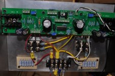
That PCB was designed as a "Swiss Army Knife" for experiments, as well as (mostly) conforming the DIYAudio UMS (Universal Mounting Spec). It has lots of connectors for resistor options, such as changing the global feedback network, cascode local feedback, FE load resistor, ... If the circuit design was totally frozen the PCB could be made much simpler and probably mounted directly to the hocky pucks.
That PCB was designed as a "Swiss Army Knife" for experiments, as well as (mostly) conforming the DIYAudio UMS (Universal Mounting Spec). It has lots of connectors for resistor options, such as changing the global feedback network, cascode local feedback, FE load resistor, ... If the circuit design was totally frozen the PCB could be made much simpler and probably mounted directly to the hocky pucks.
The swiss army configuration is part of what appeals to me. I am just getting started prototyping an F4 beast and appreciate the utility of being able to swap components and test different ideas.
Other than the swiss army aspect, its an awesome looking board. Its looks like a board you might find in a FW or PL product.
most lhquam's builds are Fugly!
Agreed. Seriously fugly.
Speculation: Perhaps Papa's change of the senst resistors from 0R47 to 1R0/6 was mainly to achieve the negative dI(fet)/dV(rail) character in improve performance for varying AC line voltages.
An alternative speculation is that 0.16 ohm gives 0.64v voltage drop at 2 x Ibias (assuming Ibias = 2A) which matches the voltage drop of the forward biased Zener pretty well. This helps in maintaining a constant bias with peak signals that push the OS into class B, i.e. where one device switches off.
BTW, congrats on completing your build. Mine is progressing rather more slowly.
 , I have 4 other amps builds to confirm
There have been some comments about the Zobel network shown in the 6Moons photos. I do not know what kind of speaker loads (or lack thereof) were causing problems without the Zobel. I found this posting by Bob Cordell which is quite informative Zobel Or No Zobel ?, as well as other postings in the thread.
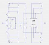
Next Challenge: Good Performance at (sanely) Low Feedback Levels:
My next goal is to modify my (spare) ZD25 PCBs for good performance at global feedback levels of around 12 dB, rather than 40+ dB of my current build. In simulations for the circuit topology below, I have found some very good parameter sets:
My next goal is to modify my (spare) ZD25 PCBs for good performance at global feedback levels of around 12 dB, rather than 40+ dB of my current build. In simulations for the circuit topology below, I have found some very good parameter sets:
Attachments
- Home
- Amplifiers
- Pass Labs
- F4 Beast Builders