The letters aP in Class aP stand for analog Pulse; which characterize operation of this type of amplification. The goals, and proposed merit/value of Class aP will follow as I explain its operation, and undoubtedly from your input.
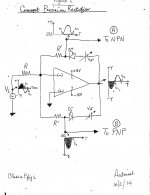
The generator of analog pulses is the Precision Rectifier [PR] shown in the schematic of the attached image. Here is how it works:
1. The operational amplifier [OA; actual is 1/2 LF353N] inverts sinusoidal input signal Vi.
2. OA has two independent and identical feedback branches emanating from its output and terminating at its inverting input.
3. Each feedback branch has a rectifying diode [actual 1N914].
4. By example of operation, allow the voltage of the shaded part of input signal Vi to increase. It follows that OA creates an inverted version at its output.
5. This step reverse-biases diode D+ of the upper feedback branch, and thus prevents input current [from the sine-wave generator] to flow through it.
6. The instantaneous voltage of the shaded input signal, and the value of input resistor R determine the value of input current moving from the sine-wave generator in the direction of the inverting input of OA.
7. This instantaneous input current [substantial in value] cannot flow in the inverting input of OA because this physical input has a high input resistance. It also cannot flow in the upper feedback branch because D+ was immediately shut off as mentioned in step 5.
8. However, this input current readily flows in the lower feedback branch because OA facilitates it by forward biasing diode D-; by using its important purpose to force zero Vdc or a virtual ground at the inverting input so as to match the actual value of zero Vdc ground of the non-inverting input.
9. Virtual ground is the electrical center point of the shaded parts of the input signal and the shaded output pulse. Both must be out of phase, and have equal;but opposite values for their voltage. This is an informal mechanism used to generate a negative pulse at output B.
10. A similar informal mechanism can be used to generate a positive pulse at output A.
11. This Precision Rectifier cuts the sinusoidal input signal [Vi] into two electrically independent mono polar pulses. Each pulse from this point forward will be processed separately. But both pulses must be processed simultaneously and identically in real time so as to recreate later on the original analog sinusoidal signal as faithfully as possible.
12. The analog pulses at the output A and B begin and end as close to zero Vdc as allowed by OA. This precise dual half wave rectification means that it is repeatable; but one needs to mind its accuracy which has to do with the faithful replication of each pulse regarding its parent portion [shaded and not] in the parent sinusoidal input signal Vi.
The next post will show a concept Class aP amplifier.
Best regards.
Attachments
I think this is Sandman class S - a circuit that splits the signal in a pos and neg portion for two output halves.
It was done with current steering; your circuit does it with voltage steering. Nice case of thinking out of the box!
You should build it, see how well it works.
Your example is with a sine wave but generally the signal is not a single sine so it is better to speak about signal splitting than 'pulse' amplification.
Edit: not Sandman class S - I will look it up.
Edit edit: A new approach to Class B, part 1 & 2, Peter Blomley, Wireless World, february/march 1971.
jan
Last edited:
Thanks Jan for your comments. I have already assembled/hard wired a dual half wave precision rectifier. I am using it in an audio power amp application for assessment. I'll gladly share all as I planned in future posts [soon] after I give additional details to further explain this approach. In reality, this approach [be it called signal splitting as you suggested, or Class aP] is operationally far from Class B; but actually one that I may call "Pulse A". The reference by Blomley is relevant to see.I think this is Sandman class S - a circuit that splits the signal in a pos and neg portion for two output halves.
It was done with current steering; your circuit does it with voltage steering. Nice case of thinking out of the box!
You should build it, see how well it works.
Your example is with a sine wave but generally the signal is not a single sine so it is better to speak about signal splitting than 'pulse' amplification.
Edit: not Sandman class S - I will look it up.
Edit edit: A new approach to Class B, part 1 & 2, Peter Blomley, Wireless World, february/march 1971.
jan
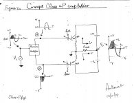
Concept Class aP amplifier
A simplified schematic of a Class aP amplifier is attached for discussion. It is in two functional parts. The precision rectifier of Post #1, and a complementary bjt power output stage demonstrator. As written, this output stage gives a trans conductance or current source power amp. Each bjt is given a mild forward bias [variable battery at base]. Here is how this amp works.
1. As the sinusoidal input voltage provided to precision rectifier goes positive [shaded], a negative rectified or pulse signal emerges at its output port B, and is presented to PNP transistor.
2. PNP amplifies shaded pulse and shows it at its collector.
3. During the time interval [0 to t1 seconds] of the start to the end of shaded negative pulse, NPN sat idle unaware of the operation of PNP. NPN did not cut off or crossover; because it was not allowed to do so.
4. At the end of time t1 of sine-wave signal, PNP returns to idle state, until a future negative going pulse comes its way for processing
5. At time t1, a positive pulse emerges at the output port A of precision rectifier.
6. It is solely presented to NPN which amplifies it during the allocated time interval of t1-t2.
7. The electrical joint at the power output [opposed collectors] splices both halves [or pulses] so as to regenerate an amplified replica of the sinusoidal input signal Vi.
8. The important result is that the bjts operated independently, equally, and were not allowed to "crossover" into each other's electrical regions of operation.
9. The business of "crossover" in Class AB power amplifiers was denied to its complementary devices; because it has already been accomplished/managed [with high precision] in the preceding line-level Precision Rectifier.
10. Point 9 above gave a clear purpose for the precision rectifier, and a clear performance objective for the power output stage.
11. Thus, each bjt is always on and operates exclusively in pulse mode A mode ; because it was denied cut off on purpose by this approach of amplification.
more forthcoming...
Attachments
")
Thank you all for your generous technical input, and encouraging comments. I thank franzm for the valuable schematics in post#9. I also commend jan didden, and franzm for their broad knowledge of amplifiers, and their acute ability to quickly recall these gems.
I am now a disciple of Blomley. I am glad to dedicate my contributions in this thread to Blomley, and Hartsuiker. Still, I will continue sharing with you my findings/understanding of their amplifier design philosophy.
Best regards.
I am now a disciple of Blomley. I am glad to dedicate my contributions in this thread to Blomley, and Hartsuiker. Still, I will continue sharing with you my findings/understanding of their amplifier design philosophy.
Best regards.
Member
Joined 2009
Paid Member
Hugh Dean (AKSA) sent me those records a couple of years ago - I believe he's studied this approach in some detail and would be a useful source of comment on this approach.
Thanks jan.didden for your interest. I will gladly oblige you, and our fellow diyaudio members.Well I for one am very much interested in your findings! I have never played with this particular topology but it should be of interest to all diy audio geeks.
Jan
Hugh Dean (AKSA) sent me those records a couple of years ago - I believe he's studied this approach in some detail and would be a useful source of comment on this approach.
Thanks Bigun. I look forward to this valuable input.
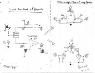
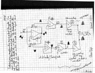
The Precision Rectifier [PR] in Post #1, maybe described as a generator of an alternative audio signal format [DC pulses]. PR can be part of an integrated amplifier, or a stand alone unit akin to a line level amplifier. The pulses are readily amplified, attenuated, and also manipulated so as to expand its scope of use. For example, the left side of the left image shows that the shaded negative pulse at output B, was inverted [via Op Amp] so as to generate a shaded positive pulse at output B'; with an equal absolute DC magnitude to that at port B.
Output pulses A, and B' are thus used to drive other power output stages which use a single polarity amplifying device; e.g. NPN [tested], and vacuum tube [expected] by example. Here is how the NPN Class aP amplifier works.
1. The bjts receive a mild idle bias.
2. The shaded positive pulse B' emerging in the time interval of 0 to t1 is first presented to the right side bjt.
3. This pulse causes a current to flow from +Vc, through the right side primary winding of the power transformer and via the collector through the bjt to ground common.
4. During this time interval of 0-t1, the left bjt sat idle, unaware of the activity of its companion.
5. The left bjt, receives next a positive [unshaded ] pulse from port A spanning the next time interval of t1-t2.
6. Collector current to the left bjt starts at +Vc, and passes through the left primary winding of the power transformer.
7. The right side bjt sat idle during this time interval [t1-t2] while its companion worked.
8. The power transformer splices the pulses, and thus regenerates a sinusoidal signal at its secondary winding for presentation to the load.
9. A proto of this bjt circuit was assembled and tested. The second right image shows its schematic, and dated back to 1998. Note how I got around "distortion" in each bjt by using Op Amps to drive their bases, and especially monitor via feedback their emitter currents for accuracy of the input DC pulses.
10. Food for thought. This is not a trick question; as I do not know its answer. Do the bjts generate harmonic distortion despite processing DC pulses and not sinusoidal [harmonic] signals. Ponder the attendant consequence if the answer is No.
More to share..
Best regards.
Attachments
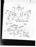
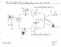
The amps described already have high output impedance. The left image shows a concept Class aP power amp of low output impedance. As you've already perceived, this approach for amplification requires using two independent amplifying devices; which maybe seen as, or is actually a detriment from the perspective of component count.
Each sub unit power amp in the schematic is the classical voltage source variety. It has bipolar power supplies, an inverting, and a non inverting inputs and utilizes overall loop feedback from its power output to its inverting ports so as to give a voltage gain of Vg. It can be commercial [abundant], or diy to suit. The amps are connected using the familiar bridge configuration. Here is how it works.
1. The shaded negative pulse at port B is first presented in real time to the inverting voltage source power amplifier.
2. This power amp then generates an amplified shaded positive pulse at its power output port which is connected to the bottom lead of the load.
3. Output current then flows out of this inverting power amp through the load and terminates at the power output port of the non inverting voltage source amp connected to the other lead of the load.
4. The output node of the non-inverting power amp has a low and close to zero impedance [due to loop feedback]. Thus, it absorbs or sinks this current emanating from the inverting power amp during the time interval of 0 to t1 seconds.
5. During the following time interval of t1 to t2 seconds, the non-inverting power amp generates next an amplified pulse [the not shaded one] at its power output node.
6. An output current then emanates from the output of the non-inverting voltage source amp, and passes through the load, and is further sunk/absorbed in the low impedance port of the inverting power amp.
7. The sequential flow of output currents from the voltage source amps are equal in magnitude and travel in opposite directions in the load.
8. Thus the load splices the pulses or regenerates the harmonic sinusoidal power output signal.
9. The right image shows the schematic of a tested proto circuit dated 1998. Two LM386N integrated low power voltage source amps are demonstrated. It works/ piece of cake wrote I!
The time is here to work with a high power Class aP power amp as a diy demonstrator.
Best regards.
Attachments
All good points. When we fast-forward to an actual implementation, I expect that the critical point will be the putting together the original wave shape* with no discontinuities or overlaps. I believe that is the main difficulty here, equivalent to crossover distortion and Gm-doubling.
*I prefer not to call it 'pulse' because it isn't - it should work on any wave shape of signals in the audio band; although class aP may be a nice marketing cry, engineering types will look through it and may even conclude you 'don't get it' and classify it with 'snake oil'.....
Jan
*I prefer not to call it 'pulse' because it isn't - it should work on any wave shape of signals in the audio band; although class aP may be a nice marketing cry, engineering types will look through it and may even conclude you 'don't get it' and classify it with 'snake oil'.....
Jan
All good points. When we fast-forward to an actual implementation, I expect that the critical point will be the putting together the original wave shape* with no discontinuities or overlaps. I believe that is the main difficulty here, equivalent to crossover distortion and Gm-doubling.
*I prefer not to call it 'pulse' because it isn't - it should work on any wave shape of signals in the audio band; although class aP may be a nice marketing cry, engineering types will look through it and may even conclude you 'don't get it' and classify it with 'snake oil'.....
Jan
The trace on an oscilloscope clearly shows that it works on any wave shape of signal in the audio band. With a sine wave from a function generator, the scope shows a string of half wave sine wave pulses instead. What is another synonym, qualifier would you prefer to use instead of pulse?. I'll take a photo [with a handheld camera] to show both traces; if successful. This endeavor is not commercial on my part; but only DIY. I got tired of sitting on this information for the last 16 years.
I am not in the business of pushing snake oil; by the circuit schematics I share, builds, and by using the tentative name Class aP. With all due respect to all DIYers, calling it Class SS for 'signal splitting' maybe or is inappropriate; despite it expected correctness from an engineering viewpoint. Best to let the name Class aP stand/slide for the time being until a third alternative is suggested and accepted. In the interim, I hope that y'all enjoy the assembly of prototypes; like the upcoming one which has a pleasing music signature.
The next 2 posts will allow you and others to probe the underlined in your note above, take scope pictures, and listen to the amp etc...
Best regards
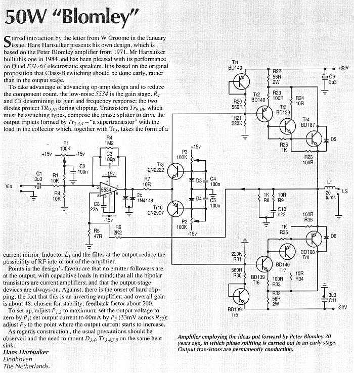
Hello jan.didden and franzm.
Did Blomley name his new approach of amplification; excluding using his [name]? Hartsuiker did not give it an engineering name either, but used the term phase splitter in his publication to describe operation.
The objection of jan.didden to the name Class aP is serious, and well-noted/taken. I have inadvertently associated this name with Class A, Class B, Class AB as distinct, apart of, or stand alone. Not so. My use of the word Class is clearly problematic. Still, I need to give this style, form, method, or type of amplification a name; any suitable name just to title this thread!
Did Blomley, and Hartsuiker [e.g. 50W "Blomley"] also attempt giving this approach an audio engineering name; if needed at all? Maybe name it PS amplification for Phase Splitting?
- Home
- Amplifiers
- Pass Labs
- Class aP amplification