Destroyer OS experiment #2
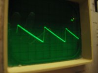
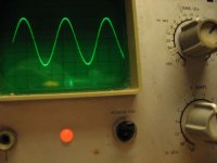
1. The right scope photo pertains to 1.5 KHz. Sawtooth with wrinkles.
2. The left scope photo pertains to 15 KHz. A cleaner sawtooth.
3. At 150 Hz, regular pulses were observed like those shown in past posts; e.g. for 15 KHz.
The capacitors in both experiments defeated the purpose of the Precision Rectifier, and corrupted the pulse signals. This corruption of pulses may also be expected in the associated aP power amp units if capacitors are present therein.
Best regards
This post deals with putting one end of the same 0.047uF PPs at the cathode of each 1N914, and connecting their other ends to common ground. The output pulses [at points A and B' of PR] for 1.5, and 15 KHz disappeared in favor of:Yes. 2>1 for same value.
1. The right scope photo pertains to 1.5 KHz. Sawtooth with wrinkles.
2. The left scope photo pertains to 15 KHz. A cleaner sawtooth.
3. At 150 Hz, regular pulses were observed like those shown in past posts; e.g. for 15 KHz.
The capacitors in both experiments defeated the purpose of the Precision Rectifier, and corrupted the pulse signals. This corruption of pulses may also be expected in the associated aP power amp units if capacitors are present therein.
Best regards
Attachments
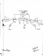
Thanks jan.didden, and Destroyer OS. I have attached 3 scope photos with the intent to continue addressing Jan's pursuit of the relevant THD analyses. Please refer to the detailed schematic of the Precision Rectifier [PR] which I am still using to drive OPTIMUS:Any capacitance anywhere near the diodes to anywhere else will destroy the HF performance and switching performance. That's basic.
Jan
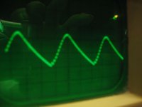
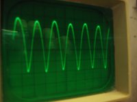
1. I connected outputs A and B' with two series connected 3.9 K resistors. A Full Wave string of pulses [15 KHz] was thus generated at the resistors' middle point; as shown in the left photo. Note that the height of adjacent pulses were not the same; maybe due to asymmetry in the generator's input sine-wave signal. How's one relate theses pulses to harmonic distortion; granted the peak height of adjacent pulses are identical?. I will derive a similar photo at the output of OPTIMUS; namely at the center point of two series connected 8 Ohm load resistors without toroid..
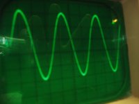
2. The phase-inverting OPA2134 [the left one in PR schematic] was reconfigured to a non-inverting buffer like the one on the right. The output pulse signals at the Op Amp outputs [15 KHz] are now out of phase, and displaced in time. The center point of the two series-connected 3.9 K resistors [between the OpAmp outs] reconstructed a sinusoidal signal. The middle photo shows the parent input signal to LF356N using the 1V/div of the scope's Y amplifier [bottom right knob]. The far right photo is the reconstructed signal at 0.5V/div; re-sized [amplified] because it came out one half the amplitude of the parent. The input and reconstructed sine-wave signals at this line-level are amenable for THD measurements.
At high frequency operation of the Precision Rectifier, a tiny error sinusoidal signal appeared [in past studies] at the inverting input of LF356N; or virtual ground. I'll show it in a future post if present.
Best regards
Best regards.
Attachments
Hm, interesting!
Jan, do you mean in general with diodes, or specifically this setup? Do you mean high frequency as in anything too low of reactance in the audio range?
You have nodes that you'll want to switch fast and clean. No cap allowed!
Jan
At high frequency operation of the Precision Rectifier, a tiny error sinusoidal signal appeared [in past studies] at the inverting input of LF356N; or virtual ground. I'll show it in a future post if present.
Best regards.
That will happen with any amp or opamp because of limited loop gain. We *assume* that the differential input across the inputs is zero but that's just a simplification. Of course, the opamp needs *some* input signal because otherwise there is no output!
")
Jan
A potential opportunity for THD measurement
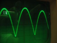
Thanks jan for your comments. I repeated the experiment I did at line-level [my last post] at the power outputs of OPTIMUS. I connected two 4 ohm power resistors [non inductive] in series between the two power output ports of OPTIMUS. Scope photos of signals at 17 KHz were then taken.
1. The left photo is the Full Wave pulse output at the center point of the two power resistors referenced to the common ground of OPTIMUS. Note that the input pulses to both power amp units were in phase; but sequential in time like those shown at the outputs of the detailed schematic of the Precision Rectifier. This power Full Wave pulse output was like that observed at line level.
2. The right photo is a reconstituted sine wave at the center point of the two power resistors. Note this time that the input pulse signals to the power amp units were out of phase and sequential in time like I reported earlier at line level. The reconstituted sine wave looks like a replica of the input signal from the signal generator. Maybe the opportunity for THD measurements is via this experimental approach
3. Curious observation regarding the display of pulses on scope via its DC or AC input selector. No change in looks either way; except for DC offset. This got me thinking to probe the influence of using external capacitors at the inputs of OPTIMUS!
Best regards
Attachments
Reading material
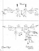
I was employed as Leather Chemist by Rohm and Haas [RandH; based in Philadelphia]; now bought up by The DOW Chemical Company. At the time, RandH's rule was to pass by its legal dept. any potential invention in any field to clear for personal use if deemed irrelevant to it. This style of audio power amplification from my hobby was not important to the business. Still, I wrote a memo to Legal explaining this invention [believed to be so at the time]. This memo [text and drawings] is attached. As you read through it, please note that I was then, like I am now a Chemist, and also a diyaudio hobbyist; but not an electrical/audio engineer. My understanding [at the time of 1998] of the common audio engineering facts, and truths I presented in this memo maybe inaccurate, obscure or downright wrong.
Best regards.
Attachments
Another loudspeaker application
I am still discussing the integrated aP amp; the schematics of which was shown in posts #28, and 29. The top part of the attached image shows a dual voice coil [DVC] woofer which is connected to the outputs of L and R OPTIMUS power amps. The resistance of each coil is 4 Ohms, and both coils bathe in a common magnetic field.
1. Note the phase of the coils.
2. The Precision Rectifier [PR] presented a ~25 mVdc output at idle to the inputs of both amps. The volume control of OPTIMUS was increased such that this input dc offset was amplified to ~0.4 Vdc at the power outputs of each. This consequently increased idle current flow by an extra 100 mA through only the NPN power output transistors for the purpose of added bias.
3. This added bias current in each power amp passes through each voice coil from the amps' output to ground. Thus, VC1 moves/pushes by convention out [up] as shown by the left bold arrow. The added and equal bias current flow through VC2 moves/pulls it by convention inward [down], and simultaneously counters the motion of VC1 such that the opposite and equal magnetic forces leave the cone centered; meaning at its resting state.
3. The sequential application of signal pulses; first to the Lch amp [0 -t1 seconds] pushes the cone out, and then during the later of [t1-t2 seconds], the Rch amp pulls the cone in; such that this combined in-out motion of the cone reconstructs the original sinusoidal signal.
The bottom figure of attached image shows another method to further push more bias current through the NPN power output transistors of both channels. It is a dual constant current source using LM337. The power input to it is at minus 8 VDC; well below the ~0 VDC baseline of the dc signal pulses at each of the amp's power output. This ensures the NPNs do not shutoff at all during operation as they process the pulses.
Note the light bulb in series with the output constant current; used as a fuse to light out at ~200 mA. I am using R= 20 Ohm which gives ~60 mA extra bias to each NPN. The heat sink [common to both power output stages] warms up acceptably with this 160 mA/ch as compared to no added bias.
Next up will be a picture of the loudspeaker.
Best regards.
Attachments
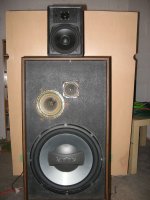
Loudspeaker application
I am not a builder of loudspeakers. But; I was able to replace the original 12" woofer which had a disintegrated surround, with a 12" dual voice coil Infinity woofer. The parent big enclosure in the photo was a hand-me-down Electro Voice model EVS 16B HiFi loudspeaker. One can still find its specs by searching Google. Its original mid range and tweeter cones have their backs sealed, and were kept in place so as to seal the enclosure. Then, I did not bother to mate the Infinity woofer with the box; but I have its T/S parameters and the internal dimensions of the box so as to calculate the enclosed performance; if needed.
The satellite loudspeaker is L300C; and oldie [1982] by A/D/S. I also replaced its woofer because its surround had disintegrated. It is a 2-way with a 4 Ohm impedance.
The image shows the diagram which integrates the two loudspeakers with each other, and with OPTIMUS.
1. The 3 hypothetical on/off switches in the diagram allow for independent listening assessments of the woofer only [2 ways], the satellite only, and the satellite with the woofer [2 ways].
2. I have both loudspeakers connected in parallel, and the center point of the woofer voice coils grounded.
3. This ensemble sounds great. I bet you still wonder how does this great sound come out of voice coils, crossover networks with their internal coils and capacitors which are fed/driven with dc pulses?
4. First, the "flow of current" through these reactive elements is and must be two way [and equal] like that from a true sinusoidal wave.
5. Second, the dc pulses are precise, and I venture to claim that they are also accurate aka like their analogous parts in the original sine waves; otherwise your ears and mine will detect irregularities in the reproduced music one's familiar with.
1. I will use this system [as a base line/reference]; but with additional dc-blocking capacitors at the inputs of OPTIMUS to unravel impact on objective and subjective performance.
2. I will substitute OPTIMUS with THRESHOLD S/150 [with no caps at its input] so as to discover the influence on performance by the 470 uF capacitor in the circuit leg of the inverting input of its diff amp.
I will gladly report the findings.
Best regards.
Attachments
If you'd like a second opinion sometime on sound, I'd plug it in.
Thank you for the offer. I hope that you and DIYers assemble and comment on their version of the amplifier, and performance. I showed ample details to put one together in a short time.
Capacitors in analog Pulse amplifcation
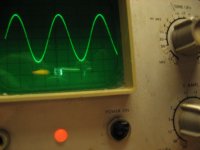
I previously noted that the shape of the analog dc pulses [origin from function generator] looked the same whether I viewed them on the scope by using its AC or DC signal select switch. I reasoned that AC coupling these analog DC pulses from the output of the Precision Rectifier to the inputs of OPTIMUS will probably behave similarly; and they did objectively.
I first listened to music[ no infinity woofer; just L300C for simplicity] by using 1uF [PP] , 10 uF [WonderCap], and 220 uF electrolytic coupling caps. I liked the sound via the 220 uF best of the three; but direct coupling of OPTIMUS was preferred overall; best relaxed.
The shape and lookon the scope of the power output half wave and full wave rectified pulses with the 220uF at the inputs of OPTIMUS were similar if not identical at 100 Hz, 1 KHz. and 16 KHz to those of dc coupling only; which I had reported earlier as scope photos.
I compared sequentially the sound of THRESHOLD S/150 [R ch] with S/150 operating in aP mode; but without input coupling caps. I preferred the sound of S/150' operating normally. However, the shape and looks of dc pulses processed at its power outputs were like those observed above and earlier for OPTIMUS with and w/o input coupling capacitors.
Still, the notion of charging and discharging a capacitor [input coupling for OPTIMUS, and a 470 uF in S/150] looms in theory to be detrimental to performance due to affecting the pulses' slewing. Pulses may rise and decay slowly and may lean to the right along the time axis.
I concluded that I could not find an objective difference due to the capacitors in the aP amplifiers just described. But, I heard a detriment to sound for the case of using input coupling caps with OPTIMUS.
The past posts covered most all of that I have on aP amplification which use therein voltage source power amplifier building blocks. The next posts will tackle Current Source aP Amplifiers.
Best regards.
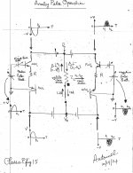
Current source aP DC amplifier
The features of this prototype amp are:
1. Complementary symmetry power output stage
2. Power outputs at zero DC common/ground reference; by using bipolar power supplies
3. Class A; because overall loop negative feedback is absent due to the nature of its current source application.
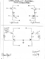
Let's assemble its simplified schematic as follows. The top part of the left image shows its simplified power output stage; a Left and Right branches of power output bjts. In an ideal world, the NPNs have identical performance, ditto for the PNPs, and the NPNs plus PNPs have identical complementary electrical properties. These power bjts sit on a tunnel heat sink with a fan blowing air through its cavity. The power resistors [R] allow the monitoring of idle current, and provide degeneration-negative feedback.
The bottom part of the image adds an independent forward bias [variable battery] to each branch. The analog pulses are in series with the batteries.
The right image adds two bipolar power supplies [A, and B of +/- 25Vdc], and two loads [Zl, and Zl'].
1. This is a bridge amplifier, and some of you may see it a Circlotron.
2. The center point of the loads Zl and Z' maybe grounded or not via switch.
3. The loads Zl and Zl' need not be identical in value. Zl or Zl' maybe equal to zero.
4. The dual polarity power supplies are the standard types. The center tap of each AC power transformer [A or B] is an independent power output node.
I'll discuss in the next post operation at its idle and with analog pulses.
The features of this prototype amp are:
1. Complementary symmetry power output stage
2. Power outputs at zero DC common/ground reference; by using bipolar power supplies
3. Class A; because overall loop negative feedback is absent due to the nature of its current source application.
Let's assemble its simplified schematic as follows. The top part of the left image shows its simplified power output stage; a Left and Right branches of power output bjts. In an ideal world, the NPNs have identical performance, ditto for the PNPs, and the NPNs plus PNPs have identical complementary electrical properties. These power bjts sit on a tunnel heat sink with a fan blowing air through its cavity. The power resistors [R] allow the monitoring of idle current, and provide degeneration-negative feedback.
The bottom part of the image adds an independent forward bias [variable battery] to each branch. The analog pulses are in series with the batteries.
The right image adds two bipolar power supplies [A, and B of +/- 25Vdc], and two loads [Zl, and Zl'].
1. This is a bridge amplifier, and some of you may see it a Circlotron.
2. The center point of the loads Zl and Z' maybe grounded or not via switch.
3. The loads Zl and Zl' need not be identical in value. Zl or Zl' maybe equal to zero.
4. The dual polarity power supplies are the standard types. The center tap of each AC power transformer [A or B] is an independent power output node.
I'll discuss in the next post operation at its idle and with analog pulses.
Attachments
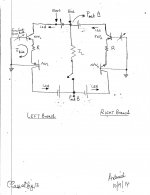
Operation of current source aP amplifier
The following two posts will explain in simple terms my view of the idle and dynamic operations of the current source aP amplifier.
The left image shows:
1. The bjts in the L and R branches idle at equal 1.2A; which is that in the prototype..
2. The load Zl is disconnected at Pout B from Pout A via the switch.
3. An arbitrary view of idle operation is. The idle current [1.2 A] starts its journey at the anode of the indicated upper left power supply battery, and sequentially passes through NPNl, R, PNPl, the bottom 2 power supply batteries, NPNr, R, PNPr the upper right power supply battery, and finally terminates at the cathode of the upper left power supply battery where it belongs.
4. Another view of idle operation is shown in the right image. Close switch so as to connect the load Zl between Pout B with Pout A. The idle current [1.2 A] circulates in the closed loop of the left branch and travels upward through Zl. Simultaneously, the idle current [1.2 A] circulates in the closed circuit or loop of the right branch and flows downward through Zl by comparison The equal and counter flow of currents through Zl nets a zero idle current through it. This also says that the voltage drop across Zl is zero Vdc. This is a simpler view of idle than in point #3, and will be used to explain pulse operation.
5. At idle, there is not a net flow of current through Zl regardless of using either view; because the L and R branch [bjts] operate in an identical manner, or are balanced.
Coming up is pulse operation which is superimposed on idle condititions.
Attachments
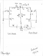
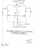
Analog Pulse Operation
The attached image is heavily populated with visual detail so as to explain the following analog pulse operation:
1. The positive pulse generator [from Precision Rectifier] is represented as a variable battery in series [additive] with the fixed positive bias battery at the input of the Left branch. The duration of this positive pulse spans the time duration of 0 to t1 seconds of the parent sine wave.
2. The shaded negative pulse generator [from Precision Rectifier] is also shown as a variable battery in series [additive] with the fixed negative bias battery at the input of the Right branch. The duration of this negative pulse spans the later time duration of t1 to t2 seconds of the parent sine wave.
3. The top NPN of left branch, and the top PNP of right branch operate in the common emitter configuration. They individually invert the phase of the input pulses as pictured at their collector nodes. Mentally join these two pulses and reconstruct an inverted sinusoidal vave at the center point of the upper dual power supply [Vo]]
4. The bottom PNP of left branch and the bottom NPN of right branch operate in the common base configuration. They individually retain the phase of their respective input pulses as pictured at their collector nodes. Mentally join their sequential [in time ] pulses so as to reconstruct the parent sinusoidal wave at the center point of the lower dual power supply at [Vo].
5. Let's now consider driving the load Zl which moves its cone. At time = 0 seconds, the idle current [1.2 A] from each branch counter flows through Zl such that its cone is at a standstill, and is not displaced or offset in either direction of movement. Note the shaded square at the bottom of Zl which signifies phase that causes cone movement due to current entering it [to left] or exiting it [to right].
5. During the time lapse [0 to t1 seconds] of the positive pulse presented to the left branch, an additional [delta i+] adds to its idle current. This added pulse current moves the cone to the left side in a pulse-piston fashion. During that same time lapse, the right branch was mostly unaware of the activity of the left branch and idled at 1.2A.
6. At time t1, the cone has returned to its center point. During the next time lapse of t1 to t2, the right branch injects an additional delta i- to its idle current. This added pulse current flows counter to that of the positive pulse, and causes the cone to move to the right in a pulse-piston fashion. During this same time interval of t1 to t2 seconds, the left branch was mostly unaware of the activity of the right branch and idled at 1.2A.
7. At time t2, the cone has returned to its center point of movement, and is poised to receive a next positive pulse etc..
The next post continues this dialog..
Attachments
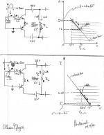
Two ways to operate the current source aP amp
The current source aP amplifier operates Class A. There are two distinct ways to drive its output stage. Allow me to set the stage as one looks at the top part of the attached image.
1. The left schematic of the top diagram shows only the Left branch of the output stage which was depicted in past posts. Therein, positive-going pulses are added in series at all times to the positive fixed bias at its input.
2. Its static and pulse operations are pictorially modeled by using or borrowing the 'electrical characteristics' of an NPN. One sees the typical pentode behavior, a load line. The cross marks the spot on the load line for idle at 1.2 A on Y [current] axis and Vc-c of 50 V [collector to collector] on the X [voltage] axis. Clearly there is another pictorial like it on the diagonal quadrant describing the operation of the Right branch driven by negative pulses.
3. The positive pulses always enable this bjt to climb up the load line to a peak value of additional current [i+p], which then falls back to idle value [1.2 A] at the end of pulse. This is one way or method to operate this output stage by sequentially maximizing the current circulating in the Left and Right branches of the output stage.. Note that Vc-c decreased at peak [i+p] operation.
4. The lower part of the image has the same drawings as above it; except the pulses which are presented to the input of the Left branch are always negative-going, and thus buck its positive fixed bias. Consequently, the pictorial of the NPN "electrical characteristic" now shows that the current circulating in this Left branch always decreases from idle [1.2 A] and slides downhill the load line for a minimum [i-], which then springs back up to its idle value of 1.2 A at the end of the negative-going pulse. This is the second way to operate the output stage; by sequentially minimizing the current circulating in the Left and Right branches.
The two ways of operating the output stage are different and thus may present different objective and subjective performance.
Attachments
Last edited:
The following two posts will explain in simple terms my view of the idle and dynamic operations of the current source aP amplifier.
The left image shows:
1. The bjts in the L and R branches idle at equal 1.2A; which is that in the prototype..
2. The load Zl is disconnected at Pout B from Pout A via the switch.
3. An arbitrary view of idle operation is. The idle current [1.2 A] starts its journey at the anode of the indicated upper left power supply battery, and sequentially passes through NPNl, R, PNPl, the bottom 2 power supply batteries, NPNr, R, PNPr the upper right power supply battery, and finally terminates at the cathode of the upper left power supply battery where it belongs.
4. Another view of idle operation is shown in the right image. Close switch so as to connect the load Zl between Pout B with Pout A. The idle current [1.2 A] circulates in the closed loop of the left branch and travels upward through Zl. Simultaneously, the idle current [1.2 A] circulates in the closed circuit or loop of the right branch and flows downward through Zl by comparison The equal and counter flow of currents through Zl nets a zero idle current through it. This also says that the voltage drop across Zl is zero Vdc. This is a simpler view of idle than in point #3, and will be used to explain pulse operation.
5. At idle, there is not a net flow of current through Zl regardless of using either view; because the L and R branch [bjts] operate in an identical manner, or are balanced.
Coming up is pulse operation which is superimposed on idle condititions.
Hi, I am following this thread with curiosity, and I congratulate with you for the initiative to bring forward a new and different idea. The bridge stage you designed is somewhat similar to one of those schematics that I presented a few months ago in this thread:
http://www.diyaudio.com/forums/solid-state/257200-two-new-output-stages-have-you-seen-before.html
with the option of having only two power battery.
Even your circuit could operate with only two batteries (suppressing a pair diagonally), but you may have a different purpose to keep all of them.
I hope that at the end you find some practical benefit (sound).
- Home
- Amplifiers
- Pass Labs
- Class aP amplification