Well in fact it is either class B (no current when no signal) or AB (small DC current when no signal) so I don't see that there should be a new class name. The concept itself is of course unique; don't know how to call it.
BTW, you can't really depend on a scope to see how well it works. The proof of the pudding is a distortion analyser to look at the residual when the fundamental is removed.
Jan
BTW, you can't really depend on a scope to see how well it works. The proof of the pudding is a distortion analyser to look at the residual when the fundamental is removed.
Jan
Thanks Jan for your constructive comments. My objective is to share a practical approach or tool of amplification with DIYers; absent at this point in time answers to your important questions, and potential relevant problems. I am glad to feel that your are interested to get to the bottom of this; thanks.
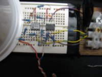
The picture on the left shows a Precision Rectifier [PR] assembled [in about 1 hour] on a proto-board. Its detailed schematic will follow come Monday. The front end OpAmp [uA741] is the inverting rectifier. Other single OpAmps are LM318, LF356, TL081CP, etc..The dark chip is a dual Burr Brown OPA2134. One half buffers the positive pulses [not shaded in past discussions], and the other half inverts the [shaded] negative pulses. RCA sinusoidal input to uA741 is shown at the bottom of the pic. The pulse outputs [same phase; but displaced in time] terminate in the EU style connector. They are transmitted via RCA cable [not shown] to a stereo DC coupled amplifier [both channels used; not shown] .
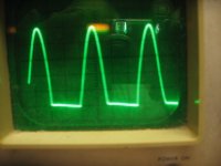
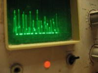
The middle picture shows the scope's trace of a 15 KHz half wave rectified pulses emanating from the [not shaded] output. The baseline of these pulses is where one finds aberrations due to crossover/switching in uA741. The right pic shows the scope's trace of Madonna doing Borderline at the same port of measurement.
Best regards
Attachments
I think what you will find is that you need a very fast and unity-stable opamp for the precision rectifier.
One of the reasons Blomley used current splitting instead of voltage splitting is that the process is inherently faster. Voltage splitting requires large voltage swings and very fast start-stopping, while in current splitting the voltage swings are much smaller. Parasitic capacitances for instances almost have no impact in current switching.
What should be interesting is how the reassembled waveform looks!
Jan
I have LM318H. It has a high slew rate of 50 V/uSec, versus uA741 of 3V/uSec. Great comparison for speed at a constant unity-gain stability for both. Another important variable is the magnitude of their open loop gain.
Will proudly show the important reassembled waveform at the terminus of power amplification.
Best regards.
Will proudly show the important reassembled waveform at the terminus of power amplification.
Best regards.
")
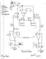
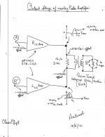
The schematic of the Precision Rectifier [PR] is the left image, and shows actual values of components. With the exception of the two resistors [15 K*], each of the others [15-20 K] maybe replaced with 10 K or lower values. Note the following:
1. The schematic was depicted earlier in simple form.
2. The string of resistors in the sequence [+15Vdc--15K*--330 Ohm at output of LF356--330 Ohm--15K* -15 Vdc ]provides a bias current [~2 uA dc] through each of the switching diodes.
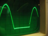
3. The middle scope picture shows a 15 KHz pulse [1 V dc peak at output A] without this bias network. Note the signal aberrations at the base line. This aberration was similarly observed by also using uA 741, and LM318H instead of LF356N.
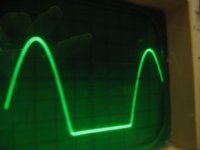
4. The scope picture on the right is that of the same signal after biasing the diodes. Its aberrations disappeared.
5. Most important is that the magnitude of the pulses before and after the application of bias was the same.
6. Best to attenuate the input signal at source; by using a dual-ganged pot [common] in the expected stereo [R and L] application.
Coming up is the fun mating it with the amplifier.
Best regards
1. The schematic was depicted earlier in simple form.
2. The string of resistors in the sequence [+15Vdc--15K*--330 Ohm at output of LF356--330 Ohm--15K* -15 Vdc ]provides a bias current [~2 uA dc] through each of the switching diodes.
3. The middle scope picture shows a 15 KHz pulse [1 V dc peak at output A] without this bias network. Note the signal aberrations at the base line. This aberration was similarly observed by also using uA 741, and LM318H instead of LF356N.
4. The scope picture on the right is that of the same signal after biasing the diodes. Its aberrations disappeared.
5. Most important is that the magnitude of the pulses before and after the application of bias was the same.
6. Best to attenuate the input signal at source; by using a dual-ganged pot [common] in the expected stereo [R and L] application.
Coming up is the fun mating it with the amplifier.
Best regards
Attachments
A DIY demonstrator of an analog Pulse Amplifier
I bought from e-Bay a stereo receiver [OPTIMUS STA-2160] for the purpose of using its pair of power amplifiers for this study. I could not find a schematic for it, so I read it from its PCB. I disabled all electrolytic capacitors in and around the signal path for each amplifier. Capacitors store charge from DC pulses and best be absent therein the amplification train. I did not bother pF valued ceramics, and the capacitor in the Zobel network at the amps' outputs. Thus,
1. I shorted across the leads of the input coupling electrolytic capacitor for pure DC coupling of the pulse signals .
2. The bias regulator for the output stage had a capacitor across it. I disabled it by cutting through its printed circuit lines.
3. Absent was the customary electrolytic capacitor in the leg of the inverting input; no change.
The left image shows the diagram of the output stage, and was shown earlier; like that using LM386 demonstrator. Note:
1. The pulse input to the power amps were connected to the detailed Precision Rectifier I showed already in the above post.
2. The power outputs are bridge-tied with a 16 Ohm power resistor in parallel with the [normally] secondary winding [12Vac at 2 Amps] of a power line toroid transformer.
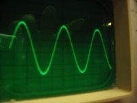
3. This load arrangement allowed the amps to put out a substantial amount of power, and further enabled viewing [with added amplification] the reconstructed sine wave Vo [15 KHz] on the scope to focus on its middle crossover section for aberrations.
4. The middle photo shows 4 Vdc peak pulses referenced to the power amps' ground seen at either power outputs. But are they really matched in amplitude which I could not tell easily. This is a concern because the voltage gain of both amps may not be exactly identical. But, there's a way to check it out and test it.?
5. The right photo of the scope's screen shows the regenerated output signal Vo = 50 Vp-p. No aberrations; e.g. crossover "distortion" was absent in its middle section in the critical higher frequency of operation which stresses the Precision Rectifier. This Vo signal has use for THD measurements.
6. The amps' common heat sink warms up substantially after a 20 minute operation under these conditions.
7. This analog Pulse amplifier is ready for music listening and/or further objective analyses.
I'll show select pictures of OPTIMUS for completeness.
I bought from e-Bay a stereo receiver [OPTIMUS STA-2160] for the purpose of using its pair of power amplifiers for this study. I could not find a schematic for it, so I read it from its PCB. I disabled all electrolytic capacitors in and around the signal path for each amplifier. Capacitors store charge from DC pulses and best be absent therein the amplification train. I did not bother pF valued ceramics, and the capacitor in the Zobel network at the amps' outputs. Thus,
1. I shorted across the leads of the input coupling electrolytic capacitor for pure DC coupling of the pulse signals .
2. The bias regulator for the output stage had a capacitor across it. I disabled it by cutting through its printed circuit lines.
3. Absent was the customary electrolytic capacitor in the leg of the inverting input; no change.
The left image shows the diagram of the output stage, and was shown earlier; like that using LM386 demonstrator. Note:
1. The pulse input to the power amps were connected to the detailed Precision Rectifier I showed already in the above post.
2. The power outputs are bridge-tied with a 16 Ohm power resistor in parallel with the [normally] secondary winding [12Vac at 2 Amps] of a power line toroid transformer.
3. This load arrangement allowed the amps to put out a substantial amount of power, and further enabled viewing [with added amplification] the reconstructed sine wave Vo [15 KHz] on the scope to focus on its middle crossover section for aberrations.
4. The middle photo shows 4 Vdc peak pulses referenced to the power amps' ground seen at either power outputs. But are they really matched in amplitude which I could not tell easily. This is a concern because the voltage gain of both amps may not be exactly identical. But, there's a way to check it out and test it.?
5. The right photo of the scope's screen shows the regenerated output signal Vo = 50 Vp-p. No aberrations; e.g. crossover "distortion" was absent in its middle section in the critical higher frequency of operation which stresses the Precision Rectifier. This Vo signal has use for THD measurements.
6. The amps' common heat sink warms up substantially after a 20 minute operation under these conditions.
7. This analog Pulse amplifier is ready for music listening and/or further objective analyses.
I'll show select pictures of OPTIMUS for completeness.
Attachments
There may be a significant difference between the original Blomley's amp and the implementation as done by Hartsuiker.
Blomley drives the splitter at quite a high impedance provided by Tr3 and Tr6 (1 mA quiescent current) as Hartsuiker drives it at low impedance, slightly above 10 Ohm.
Blomley drives the splitter at quite a high impedance provided by Tr3 and Tr6 (1 mA quiescent current) as Hartsuiker drives it at low impedance, slightly above 10 Ohm.
There may be a significant difference between the original Blomley's amp and the implementation as done by Hartsuiker.
Blomley drives the splitter at quite a high impedance provided by Tr3 and Tr6 (1 mA quiescent current) as Hartsuiker drives it at low impedance, slightly above 10 Ohm.
Thank you for your comments. Interesting that Hartsuiker named his amp a 50W Blomley; despite the functional differences you noted. We've seen the detailed schematics of Blomley and Hartsuiker; thanks to franzm. Does the demonstrator amp I presented in my previous post rise to the stature of naming it a "Blomley"; for any reason?
Interesting and good progress!
Some comments:
I think the biasing of the PR circuit is critical to low distortion. You may want to come up with some scheme to adjust the bias for both sides with a single pot to look at the results on a THD analyzer;
Your initial test with the Optimus output stages is nice to give an initial result, but once you go in deeper with a distortion analyzer it will be hard to separate the effects of the PR/Blomley concept from the aberrations of the Optimus part.
Jan
Tips for trouble-free operation
A great design feature in OPTIMUS, is a fuse [6A fast] at each power output. I lowered each to 4A fast. It is important to insert initially a series 2A fast in one leg of the loudspeaker for its protection; especially if working with proto-board. With past use, its sockets, may have become aberrant, loose, and may even spontaneously open, and I have seen ICs pop out in operation.
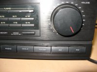
Another good feature in OPTIMUS is its volume control as shown in photo. I used it. I always start at its minimum setting and advance it slowly. In the original design of OPTIMUS this volume control was ahead of its tone amp. The tone amp was bypassed, and this volume control relocated to the RCA inputs; or the non-inverting input of both amps.
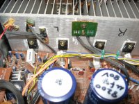
A photo of the power output bjts on a common heat sink is shown. On it is a dual bias regulator [green] and 3 methods to shut off the amps at high temperature operation of the heat sink. I did not disturb these functions.
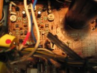
A third photo shows the front-end of the power amps. One can pick out the DC blocking caps which were shorted on the underside PCB. The white trim pots are for DC offset adjustments at the power outputs. The diff amp of each channel [NPN] is packaged in a black chip; three leads on either side of it.
For this set up up,
1. I fire up the Precision Rectifier first, and measure DC voltage at it outputs [A, and B'] to confirm its established DC offset of ~+25 mV.
2. Initial OPTIMUS status, is power off, min volume control setting, speaker on/off switch in off position [great feature]. NO load.
3. Turn power on to OPTIMUS. Enable speaker outputs. Measure the voltage at either power out relative to common, and importantly the bridging DC offset [~100 mV dc]. Advance volume control, and continue to monitor output voltages to confirm no unreal DC voltage offsets exist.
4. Connect the fused load.
Best regards
A great design feature in OPTIMUS, is a fuse [6A fast] at each power output. I lowered each to 4A fast. It is important to insert initially a series 2A fast in one leg of the loudspeaker for its protection; especially if working with proto-board. With past use, its sockets, may have become aberrant, loose, and may even spontaneously open, and I have seen ICs pop out in operation.
Another good feature in OPTIMUS is its volume control as shown in photo. I used it. I always start at its minimum setting and advance it slowly. In the original design of OPTIMUS this volume control was ahead of its tone amp. The tone amp was bypassed, and this volume control relocated to the RCA inputs; or the non-inverting input of both amps.
A photo of the power output bjts on a common heat sink is shown. On it is a dual bias regulator [green] and 3 methods to shut off the amps at high temperature operation of the heat sink. I did not disturb these functions.
A third photo shows the front-end of the power amps. One can pick out the DC blocking caps which were shorted on the underside PCB. The white trim pots are for DC offset adjustments at the power outputs. The diff amp of each channel [NPN] is packaged in a black chip; three leads on either side of it.
For this set up up,
1. I fire up the Precision Rectifier first, and measure DC voltage at it outputs [A, and B'] to confirm its established DC offset of ~+25 mV.
2. Initial OPTIMUS status, is power off, min volume control setting, speaker on/off switch in off position [great feature]. NO load.
3. Turn power on to OPTIMUS. Enable speaker outputs. Measure the voltage at either power out relative to common, and importantly the bridging DC offset [~100 mV dc]. Advance volume control, and continue to monitor output voltages to confirm no unreal DC voltage offsets exist.
4. Connect the fused load.
Best regards
Attachments
Interesting and good progress!
Some comments:
biasing of the PR circuit is critical to low distortion.
Your initial test with the Optimus output stages is nice to give an initial result, but once you go in deeper with a distortion analyzer it will be hard to separate the effects of the PR/Blomley concept from the aberrations of the Optimus part.
Jan
Thanks Jan for your encouraging comments. Forward bias to the 1N914 diodes in Precision Rectifier [PR] is very critical; so as to rid the output pulses from aberrations in their baseline as shown in a past post. With and without diode bias is readily discernible by listening tests. The bias current through the 1N914 diodes can easily be increased [50-100 uA nominal] with decreasing values of the two resistors labelled K*. I've also used current sources instead of the K*resistors e.g from 2N3819 JFET which were hand-matched.
Here is a starting point for an approach to address the second THD concern in your post above; which is to define a comparative control circuit as follows:
1. Mentally, pluck out the LF356N circuit only from the integrated aP amplifier.
2. Join the inputs of OPA2134 at the formerly points A and B'.
3. Feed the same sine-wave signal to this joined input of OPA2134; granted, the right buffer's non-inverting input [pointA] is thus allowed a bias path to common.
4. A common bridge amplifier is obtained which has all of the functional blocks; less PR, and its attendant DC output offsets.
5. The output signal Vo [toroid output] of this common bridge amplifier is then compared with the input sine-wave source signal. In addition, the power output signals referenced to ground [without toroid] are also used to understand the impact of the "toroid tool" on the signal.
6. Ditto for the integrated aP amplifier [with toroid]; with a one on one followup comparison of results; [meaning experiments 6 versus 5].
7. The same toroid may be used in a voltage step down mode in another set of comparative experiments.
8. I do not have a THD analyzer, and a dedicated scope camera.
9. But; a dedicated scope camera allows one to first take a picture of the input signal. Print it on a transparency. Then take a picture of Vo; attenuated, and sized to that of the input signal by using the scope's vertical adjustments. Print it on the same or a second transparency. Superimpose the transparencies in a good light to judge.
Best regards
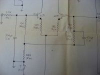
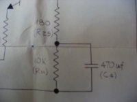
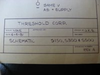
I own a THRESHOLD S/150 which I bought in the early 1980's. Works great. Then, I asked Mr. Pass [via hand-written letter] while he was still at THRESHOLD Corp. for its schematic. He [kindly] sent me a draftsman original; like a map in size. Its drawing record is shown in the attached photo. Also shown is a photo of the front end diff amp schematic, and a third photo with focus on the electrolytic capacitor [470 uF] shown along the leg of the inverting input. This capacitor is still in the circuit of each of its two amps.
I have already used it like I did with OPTIMUS for music assessment, and with sine-wave input signals. I will plug it in the aP configuration instead of OPTIMUS, and collect DC measurements, and scope photos to post. This repeat question probes the influence of the 470 uF [times two] on objective and subjective tests.
S/150 has fuses at it power outputs [originals, and untouched]. Its power outputs are banana-jack style; very useful as on/off speaker switches for measuring DC offsets prior to connecting the load.
Best regards
Attachments
Consider what happends when a reactive load is driven. The zero crossing of Voltage does not occur at the same time as the zero crossing of the Current. This means that the current crossover occurs at a time when one or the other output buffer is trying to hold it's side of the load at zero volts. Depending on the damping factor or output impedance of the buffers, an error signal will be present at the output of the inactive buffer.
Will this be any different than what happends when a conventional power stage drives a reactive load? At some point in the waveform other than at zero volts the load current must reverse direction and the other output device(s) must deliver current to the load. In a class A output stage, current is already flowing in both output devices so the transition is seamless (we hope). Again the damping factor plays a role.
When the load is driven by current sources, the load must be allowed to assume whatever voltage it wants with no disturbance to the current waveform. A damping resistor of perhaps 50 Ohms may be connected in parallel with the load.
Thank you Loudthud for your analyses and thoughts. This demonstrator OPTIMUS aP amplifier readily drives an unenclosed MCM 15" semi full-range, a 2-way [L300 C], and a 3-way [L-730] A/D/S loudspeakers without problems; like unusual sounds, buzzes, oscillation etc; when using familiar music. Each loudspeaker sounds great, and has a detailed clear performance. This amp's good sounding music [to my ears], and its electrical well-behavior are my reasons for sharing its style of amplification with the diyaudio community.
Best regards
Best regards
It looks fun.
Why don't you have any decoupling for the diodes? Will it cause an issue? (I didn't study it to hard)
Hello Destroyer OS. Maybe you mean put a capacitor across each, or a capacitor from each's cathode to ground or virtual ground. I will do this experiment;[did not do before]and initially use small film capacitors and report back.
Best regards
Destroyer OS experiments of previous post
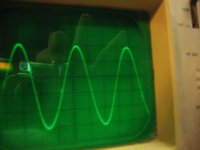
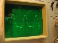
1. Left scope photo is for 150 Hz output signal [at points A or B']; a distorted sine wave.
2. Right scope photo is for 15 KHz output signal; a clean-looking sine wave. In this case, the ac impedance of 0.047uF [225 Ohms] allowed LF356N to operate like a standard inverting amp; meanining as if the diodes were not in circuit.
I will show 2 posts for the 2 independent experiments. This post deals only with putting a 0.047uF polypropylene cap across each 1N914 diode in Precision Rectifier [PR]. The pulses shown in past posts at outputs A and B' of PR disappeared in favor of:Yes. 2>1 for same value.
1. Left scope photo is for 150 Hz output signal [at points A or B']; a distorted sine wave.
2. Right scope photo is for 15 KHz output signal; a clean-looking sine wave. In this case, the ac impedance of 0.047uF [225 Ohms] allowed LF356N to operate like a standard inverting amp; meanining as if the diodes were not in circuit.
Attachments
- Home
- Amplifiers
- Pass Labs
- Class aP amplification