would these circuits work? one's a combination of zen & sen to be used with single supply.
the one on the right is that plus bjt unbalancer.
i want to use them with tda1387- output current of about 0.5mv i believe..
the one on the right is that plus bjt unbalancer.
i want to use them with tda1387- output current of about 0.5mv i believe..
An externally hosted image should be here but it was not working when we last tested it.
Last edited:
I believe in the righ size circuit the low JFETs are in CCS function; only high side JFETs change conduction/amplify the input signal. So if we use a PNP for low side, the emitter will oppose against the output signal, because base will be at a fixed potential (source from low side JFETs). In other words, will reduce the out signal and distorts it. The low side NPN version will serves a "loose" CCS but ideal is to define things with base reference (like some diodes) and use a emitter resistor to define the output current (making a "conventional" diode-biased CCS). These bipolars will become a single-ended buffer, with signal flowing in high side NPN.
If you don't use this DAC with low impedance loads, and not use with long cables, you can use the left side circuit. Really is a sort of "single-ended ZEN".
If you don't use this DAC with low impedance loads, and not use with long cables, you can use the left side circuit. Really is a sort of "single-ended ZEN".
Thank you. How about this one? Back to complimentary bjts. Sorta half diamond buffer? Maybe it can be called zenmond. X-D
that is if it works...
that is if it works...
An externally hosted image should be here but it was not working when we last tested it.
Interesting proposition, but unfortunately one/two problem exists: the JFETs will be subjected to only about 0.6V or so, so they will be starved. And the BJTs will be subjected to a enourmous/heavy base bias, so they will conduct a lot of current and will overheat.
In fact, simple circuits like Zen/Cen/Sen are beautiful but not lend themselves to easy modifications... just because they are so simple, one simple part change and behaviour change, sometimes drastically.
In fact, simple circuits like Zen/Cen/Sen are beautiful but not lend themselves to easy modifications... just because they are so simple, one simple part change and behaviour change, sometimes drastically.
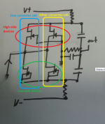
how about this one, tho?
differential dac input. if it can work, which one's flipping the phase?
differential dac input. if it can work, which one's flipping the phase?
An externally hosted image should be here but it was not working when we last tested it.
Only if DAC chip have same current offset from JFETs and have same output polarities - some are current unbalanced but is hard to match with the JFET, and loses precious current with loss os precious JFET transconductance. This means in practice one can use the "entire" ZEN I-V for each DAC output phase. Of course we will have 2 outputs (maintain balanced operation).
About output, will be tricky/picky to proper use even with emitter resistors, unless one use high values like 500 ohms to prevent BJT meltdown and loss of JEFT drain voltage, but so this results in rather high output impedance, negating most of the follower benefits...
About output, will be tricky/picky to proper use even with emitter resistors, unless one use high values like 500 ohms to prevent BJT meltdown and loss of JEFT drain voltage, but so this results in rather high output impedance, negating most of the follower benefits...
how about this? we completely eliminate the -v side of the circuit. apologies for the crudeness but i only wanted to clarify the concept, as if it isn't simple enough already.
let's say the jfets aren't even paralleled. how would it perform compared to the original zen i/v? double the distortion?
let's say the jfets aren't even paralleled. how would it perform compared to the original zen i/v? double the distortion?
An externally hosted image should be here but it was not working when we last tested it.
Last edited:
Only one side JFET will work only with DAC chips with enormous current offset, and I don't know one with such high current. For offsetting this current we put one JFETs on low side for each high side JFET, resulting in original circuit ")
Using one JFET "per high/low side" instead a pair (resulting in one JFET for high side and one JFET for low side) results in higher input impedance, and for me works flawlessy for several DAC chips, like TDA1541 or AD1860 and cousins.
Using one JFET "per high/low side" instead a pair (resulting in one JFET for high side and one JFET for low side) results in higher input impedance, and for me works flawlessy for several DAC chips, like TDA1541 or AD1860 and cousins.
Im sorry here i gotta scratch my thick skull.
Could you please elaborate on high/low design?
Are you saying that you simply split the original zen i/v?
Wouldnt they recombine when fed from the same output of a dac tho?
Im using it with tda1387 so your method might be the ticket i need
Could you please elaborate on high/low design?
Are you saying that you simply split the original zen i/v?
Wouldnt they recombine when fed from the same output of a dac tho?
Im using it with tda1387 so your method might be the ticket i need
Some concepts at attached image.
The TDA1387 have a 1mA output offset, resulting very low current to use only with high side JFETs only, even if with only one JFET (one cell). Maybe this will work but with far-reduced performance.
So one can use high+low side as always, but is good to check the resulting voltage offset in TDA output pin and to check resulting JFET drain voltage. My adjustable MOSFET option can be adjusted for desired voltage offset. Of course, the adjustment can be applied to JFET version. The TDA1387 supports 0V to 1/6VDD voltage offset in their output pin. Or probably 1mA will not change things too much: experiment with "original" first. For alternative DACs using JFETs, search on ZEN-CEN-SEN thread (http://www.diyaudio.com/forums/digi...-evolution-minimalistic-iv-converter-183.html). In this thread probably one can find most resources about the JFET version/variants, since some members probably will be using chips like TDA1387.
PS.: I don't mention one thing yet: since low side devices in your drawing are N-channels, these don't contribute to AC output. You can dispense the "low side" capacitor and use only one attached to "V+" side, and gain a little output voltage. But is good to maintain the "low side" resistor (the resistor to V-) to better equate low side/high side JFETs dissipation.
Attachments
Last edited:
Thank you, i sort of understand. The 'zen' like design would certainly be economical for me since i can use 117 instead of 170.
Do you think the performance will be significantly lacking compared to zen iv? Ill be building the single ended design soon but wont have the zen to compare for a while.
Do you think the performance will be significantly lacking compared to zen iv? Ill be building the single ended design soon but wont have the zen to compare for a while.
http://www.firstwatt.com/pdf/art_zen_iv.pdf
The Nelson Pass D1 I/V is made with single-ended operation. My MOSFET design is a sort of "D1 push-pull version". JFETs will work in Single Ended too. Only "second harmonics" will rise versus the push-pull version, not much if one measures the resulting drain voltage (rules more or less like the original ZEN).
The Nelson Pass D1 I/V is made with single-ended operation. My MOSFET design is a sort of "D1 push-pull version". JFETs will work in Single Ended too. Only "second harmonics" will rise versus the push-pull version, not much if one measures the resulting drain voltage (rules more or less like the original ZEN).
thanks your excellent work.
For those of you looking for the silver bullet to input impedance concerns, this is how it is implemented on my board - The amplifier is not in the audio path. It reduces the input impedance from 10-15 ohms to less than 1 miliOhm (~0.0005 ohms or so) as drawn!
I have included a picture of the original version that uses followers instead of an amplifier to accomplish the same thing if adding the amp takes away too much from the Zenness.
The amp version also brings the jfet offset inside the loop to keep input offset at essentially zero. Secondarily, putting the offset voltage you need into the + amp input is all you have to do for DACS like the 1543/5 and Sabre!
Adjust the voltage, resistors, and/or number of jfets as in the article and other posts for the DAC you have...
Dave

Hi Greedy Boyzzzz,
Is Zen I/V stage suitable for this board?
JE Labs: nos TDA1541 tube DAC
hHw can I manage the voltage gain?
Thanks
Is Zen I/V stage suitable for this board?
JE Labs: nos TDA1541 tube DAC
hHw can I manage the voltage gain?
Thanks
Hey all I know I am a number of years late to the party, so thanks for understanding
Also Hi Nelson!
Did the D1 simply feature a gentle frequency roll-off as per NP's graphs in 2010, or did the D1 also feature a lowpass filter after the I/V stage?
I'm building my first DIY DAC right now and looking hard at the Zen I/V. If I understand correctly, I may be able to tweak values so that it acts as an I/V AND a lowpass filter?
The D1 operated by sending the outputs of the balanced PM63's to
Common Gate Fets (essentially cascoding the output of the DACs).
There are single-pole filters (cap to ground) at the output of the DAC chips
and then another pole (cap to ground) at the Drains of the Common Gate
Fets. Those signals go to Fet followers and then to the outputs.

Common Gate Fets (essentially cascoding the output of the DACs).
There are single-pole filters (cap to ground) at the output of the DAC chips
and then another pole (cap to ground) at the Drains of the Common Gate
Fets. Those signals go to Fet followers and then to the outputs.
Hi, I am exploring possible I/V circuits for PCM1796 dac I am planning to build. Many years ago, I think Papa mentioned that for PCM1794 which has similar characteristics that one could use a single ended common gate circuit biased through the dac directly. Further down the thread it was also mentioned that D1 in single ended config can be modified to suit the dac. My knowledge in electronic circuits is too basic to understand the differences between what Papa mentioned and using D1 directly, especially the part on biasing the common gate circuit "through the dac directly". Hope someone can be kind enough to enlighten me. Thanks.
Best regards
Liu
Best regards
Liu
- Home
- Amplifiers
- Pass Labs
- Zen I/V Converter