TMC (Transitional Miller Compensation) is a variant of two pole compensation and it's used to achieve higher slew rates at lower frequencies (like the audio frequencies), it is a form of compensation proposed by Cherry and modified by Peter Baxandall, it's called transitional because for lower frequencies the impedance of the 2nd capacitor is higher in it's absolute value when compared to the impedance of the resistor, for higher frequencies the second capacitor has a impedance lower than the resistor in module and the compensation network begins to act like common Miller compensation scheme, the peaking is caused by a pair of complex poles at the output EFs, with simple Miller compensation it appears too. TMC is not unstable see the threads of my MOSFET amplifier and the Honey Badger by Peter V (ostripper) or you can consult Bob Cordell's book, chapter 9 (Advanced forms of Compensation), page 182.
Daniel
with the values you use (68pf/1KR) the transition frequency is 2.3MHz, and that is the problem I see with your compensation network.
TMC for not causing problems the transition frequency must be lower. If TMC is done correctly there is no problem.
Hi Sergio and thank you very much for your help,
I will try to reduce the open loop frequency cutoff between 500kHz and 1 MHz, I think you're right with all this open loop bandwidth the amplifier is less stable. What you suggest me to do? Increasing the value of c1 to 100pF and c2 to 470pF is a good idea?
Best regards,
Daniel
I will try to reduce the open loop frequency cutoff between 500kHz and 1 MHz, I think you're right with all this open loop bandwidth the amplifier is less stable. What you suggest me to do? Increasing the value of c1 to 100pF and c2 to 470pF is a good idea?
Best regards,
Daniel
I think you not fully understand what I said, The 2.3MHz is the frequency at which the capacitor from the compensation network will have the same impedance as the resistor from the compensation network, you have to increase the value of the resistor and decrease the capacitor.
try 2k, 220p, and 22p for Cmiller. the transition frequency will be 350k from the output stage to the vas.
when possible to post attachments, I will send some ideas for dealing with the peaking.
Your open loop frequency cutoff is OK.
try 2k, 220p, and 22p for Cmiller. the transition frequency will be 350k from the output stage to the vas.
when possible to post attachments, I will send some ideas for dealing with the peaking.
Your open loop frequency cutoff is OK.
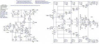
Have change your base stopper resistors values, the compensation network. Add c14, c15 for addressing the problem of the peaking at high frequency and for stability at the output stage.
Have change the bias spreader because the drivers transistors q9, q10 are not in the heat-sink. Have change the output zobel network, and add a speed capacitor (c16).
A headphone amplifier don´t need output inductor. And is better to add some capacitors at emitter of Q16/Q17 to ground.
the distortion at 20Khz / 2V rms in 32 ohms is 0.0001%, and at 1khz is 0.000005% !!!
See if you like it")
Have change the bias spreader because the drivers transistors q9, q10 are not in the heat-sink. Have change the output zobel network, and add a speed capacitor (c16).
A headphone amplifier don´t need output inductor. And is better to add some capacitors at emitter of Q16/Q17 to ground.
the distortion at 20Khz / 2V rms in 32 ohms is 0.0001%, and at 1khz is 0.000005% !!!
See if you like it
Attachments
Last edited:
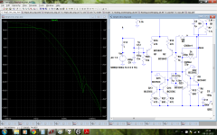
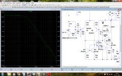
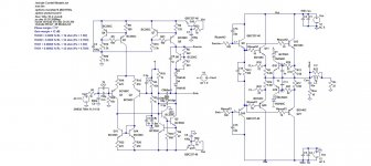
first image is the close gain with the complex mirror in input stage.
the second with the simple mirror.Everything else is equal.
As you see the complex mirror can have more negative aspects than positive. The simpler the better in my view
the second with the simple mirror.Everything else is equal.
As you see the complex mirror can have more negative aspects than positive. The simpler the better in my view
Attachments
Hi Sérgio,
Thank you very much for your help, great improvements, lower resistors at the output transistors for faster response, base to collector capacitors to parallel with cbc (to decrease bandwidth of the driver transistors and reduce the chances of oscillations).
About the input stage current mirror I think you can be right that transistor could be adding a pole that is causing the peaking, maybe it's better remove it. I don't see the purpose of Vbe multiplier + diodes, I prefer using only a vbe multiplier, why you use this two technics? that's weird. Try to add a capacitor with 2.2pF between the IPS output and VAS output similar to a dominant pole capacitor to improve 1-20kHz phase margins and reduce the peakings at those frequencies.
Do you think I should also try this compensation values for my MOSFET amplifier?
And about remove the helper transistor at the current mirror?
I have the open loop 0dB point at 2.7 MHz in my MOSFET project, but I've no peakings, what do you think?
Best regards,
Daniel
Last edited:
I've simulated the circuit now, and I think that a phase margin of 62º it's not very good it's better to raise it to 65º or more, try a small capacitor (1-10pF) in parallel with R3, try also BTMC you can find it in my MOSFET amplifier thread. The lack of phase margin is caused by the poles introduced by C14/C15 and that's normal.
Best regards,
Daniel
Best regards,
Daniel
Last edited:
If you use your vbe multiplier you will overcompensate the temperature change of the output transistors, It means that when the output transistors start to get hot the quiescent current of the output transistors start to drop to much and the distortion increase, adding the diodes is very important for the quiescent current to stay more constant and less distortion.
If the drivers transistors where mounted in the heat sink the diodes where not necessary,
But of course the best way to learn is making mistakes, so go ahead and use a simple vbe multiplier
If the drivers transistors where mounted in the heat sink the diodes where not necessary,
But of course the best way to learn is making mistakes, so go ahead and use a simple vbe multiplier
Hi Sérgio,
If you say so maybe I should use that compensation scheme.
Because I only have thermal tracking for the output transistors not for the EF drivers, and I think I understood what you're are doing with that bias spreader. The diodes are for the EF driver stage and the vbe multiplier to attach to the heatsink for temperature compensation of the BD1xx devices, know after your explanation it makes sense to me.
Can you give me some ideas of what I should improve in my MOSFET amplifier? Please.
Best regards,
Daniel
I've simulated the circuit now, and I think that a phase margin of 62º it's not very good it's better to raise it to 65º or more, try a small capacitor (1-10pF) in parallel with R3, try also BTMC you can find it in my MOSFET amplifier thread. The lack of phase margin is caused by the poles introduced by C14/C15 and that's normal.
Best regards,
Daniel
Yes of-course put a 2pf capacitor in parallel with R3 to compensate the input transistor capacitance.
And if you exclude the helper transistor from the mirror, you can decrease C14/15 as low as 27pf, that 2 measures will make the phase better than 70º for sure.
Can you give me some ideas of what I should improve in my MOSFET amplifier? Please.
Best regards,
Daniel
One thing that you have to change is the constant current sources, the feedback ccs is not very good for this, because current varies to much with temperature.
If you want to make a simulation with temperature changing from 0º to 100º in ltspice use ( .step temp 0 100 10 )
Do you think I should also try this compensation values for my MOSFET amplifier?
And about remove the helper transistor at the current mirror?
I have the open loop 0dB point at 2.7 MHz in my MOSFET project, but I've no peaking, what do you think?
Best regards,
Daniel
You have no peaking because your output stage is slow and is masking the problem. remove that transistor.
You have to think about thermal drift. the vas current source is changing from 7,8ma to 10,8ma with temperature changing from 0º to 100º, you have also to compensate the driver transistors.
And make the quiescent output current 100mA , that is the zero tempco
from lateral mosfet.
I like the bootstrapping drivers and input stage, interesting.
Try to learn more about error correction, its a very good technique to make the output stage more linear, especially hawksford error correction. I have my one way to implement the hawksford error correction, I do not like very much the way Bob Cordell does.
Last edited:
Hi Sérgio, thank you very much for your help, 
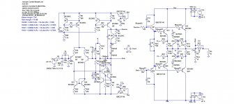
I've removed the helper transistor from the input stage current mirror, I've also added a little 3.3 pF capacitor in parallel with R3 and to finish I've added a 2.2 pF capacitor in the compensation network to have a BTMC scheme, this compensation scheme has more phase/gain margin when compared to a simple TMC scheme, it also removes the peaking and lack of phase margin present at 1-20kHz frequency range improving the amplifier stability.
I've also reduced C14 and C15 to 33 pF. Using the previous TMC scheme 68 pF/68 pF / 1K, I think I have also a good stability, what do you think?
I don't know very much about Hawksford error correction but it seems very interesting, could you please show me your variant?
Where I can learn about Hawksford error correction methods?
What do you suggest me to use as current sources for my MOSFET amplifier?
I thought that the feedback current source is one of greatest current sources, the Honey Badger uses it. How I can do the thermal compensation of the driver?
What you suggest me to use?
PS: I've attached the LTSpice circuit for my MOSFET amplifier, with the last changes
Best regards,
Daniel
Attachments
-
 Amp7_btmc_hb5_s_bd12_prot.jpg225.6 KB · Views: 116
 -
BC3x7_40 Models.txt1.2 KB · Views: 29
-
Cordell Models.txt20 KB · Views: 21
-
Amp5_btmc_imp_v5.asc15.5 KB · Views: 25
-
Amp5_tmc_imp_v4.asc15.3 KB · Views: 29
-
 Amp5_btmc_imp_v5.jpg178.1 KB · Views: 122
 -
 Amp5_btmc_imp_v4.jpg187.9 KB · Views: 132
 -
Amp7_btmc_hb5_s_bd12_prot.asc27.4 KB · Views: 30
- Status
- This old topic is closed. If you want to reopen this topic, contact a moderator using the "Report Post" button.
- Home
- Amplifiers
- Headphone Systems
- Simple Headphone's Amp for beginner