decayed.cell - I may very well do another run at some point and post them over in the vendor's bazaar subforum if all continues to go well with testing. I'll let you know if I do. I agree, it would be good to have the panels available as a set with the PCB. One of the big plusses of this amp - as with the O2 - is the matching case and that isn't of much use without the drilled panels.
It also turns out that Seeed Studio has a 5 board option (quantity) for the 4 layer PCB fab service if anyone wants to fab some of their own with those 4-layers Gerbers I posted Their selector comes up with a default quantity of 10, but there is a 5 qty option in the pulldown menu. I think that worked out to be around $100 for 5 PCBs plus $20 DHL express, vs. $120 or so for 10 PCBs with $30 DHL express. The 10 are the lower cost-per-board, but 5 shaves $30 off the total cost.
Erik - the outfit is Proto Panel:
http://protopanel.com/products-services/custom_front_panels_milling_50_discount.aspx (opens web page)
They claim to have the discount going on through the end of the month.
Last edited:
mrsavage - I'm using Cadsoft Eagle, here:
CadSoft EAGLE PCB Design Software - EAGLE Support, Tutorials, Shop
https://www.cadsoftusa.com/buy-eagle/?language=en
The free (for non commercial DIY only) "light" version goes up to 80mm x 100mm, the size of the O2 amplifier, with 2 layers maximum.. The other for-pay versions allow more layers and bigger boards.
Definitely recommended to give it a try!") Essentially you build up a schematic first using the schematic editor, then hit a button and it brings up the PCB editor with all the parts sitting in a pile at the bottom that then have to be placed. From then on any changes to the schematic - adding or deleting parts - track on the PCB board. Moving stuff around on the PCB editor has no effect on the schematic editor.
Essentially you build up a schematic first using the schematic editor, then hit a button and it brings up the PCB editor with all the parts sitting in a pile at the bottom that then have to be placed. From then on any changes to the schematic - adding or deleting parts - track on the PCB board. Moving stuff around on the PCB editor has no effect on the schematic editor.
Probably the best way to get started learning is do a search on You Tube for "CADSOFT EAGLE". A few outfits have done very good multi-part videos explaining all the basics. Eventually you will need to create and add parts to the stock libraries. That turns out to be easy.
I'm having a lot of fun with Eagle. It is really amazing this level of computer power just sits on the desk in a laptop now. When I last laid out integrated circuits and microwave stuff a long time ago it was on ComputerVision CAD machines, early Sun Workstations, and Mentor Graphics Workstations that probably had about the same compute power as a pocket calculator today. I managed some engineering groups later on but didn't get hands on with the more recent design tools, just signed the checks.
CadSoft EAGLE PCB Design Software - EAGLE Support, Tutorials, Shop
https://www.cadsoftusa.com/buy-eagle/?language=en
The free (for non commercial DIY only) "light" version goes up to 80mm x 100mm, the size of the O2 amplifier, with 2 layers maximum.. The other for-pay versions allow more layers and bigger boards.
Definitely recommended to give it a try!
Essentially you build up a schematic first using the schematic editor, then hit a button and it brings up the PCB editor with all the parts sitting in a pile at the bottom that then have to be placed. From then on any changes to the schematic - adding or deleting parts - track on the PCB board. Moving stuff around on the PCB editor has no effect on the schematic editor.Probably the best way to get started learning is do a search on You Tube for "CADSOFT EAGLE". A few outfits have done very good multi-part videos explaining all the basics. Eventually you will need to create and add parts to the stock libraries. That turns out to be easy.
I'm having a lot of fun with Eagle.
It is really amazing this level of computer power just sits on the desk in a laptop now. When I last laid out integrated circuits and microwave stuff a long time ago it was on ComputerVision CAD machines, early Sun Workstations, and Mentor Graphics Workstations that probably had about the same compute power as a pocket calculator today. I managed some engineering groups later on but didn't get hands on with the more recent design tools, just signed the checks.
Last edited:
You can open any eagle file as long as you have the same or a higher version, no matter
what version (free, student, pro,etc...) created it. You might not be able to edit it, but you can view it. Just download the files to a directory on your computer, open EAGLE and
do File>open>schematic and navigate to where you put the downloaded files.
what version (free, student, pro,etc...) created it. You might not be able to edit it, but you can view it. Just download the files to a directory on your computer, open EAGLE and
do File>open>schematic and navigate to where you put the downloaded files.
You will need two more files that I haven't posted, the schematic (.sch) and PC board (.brd) files. The Gerber files that go out to fab (the ones I posted) are something that you can tell Eagle to create. You can even view those with a Gerber viewer like this one:
Online Gerber Viewer
If you are using the free version of Eagle it would choke on the 80x160mm size and 4 layers of this "ODA" amp design. Go on over to the parallel LME49990 amp thread and I'll post the .sch and .brd files for the 2 layer version of that one. It is just 80x100mm and should work with the free Eagle.
You will probably get some complaints from Eagle upon loading the files due to missing libraries. I had to create the library parts for LME49990, the jacks, the rotary switch, and a few other things. But at least it should load what it can and let you mess around with it. Creating those parts from the data sheet information and adding them back into Eagle is a good way to learn how the libraries work.
Online Gerber Viewer
If you are using the free version of Eagle it would choke on the 80x160mm size and 4 layers of this "ODA" amp design. Go on over to the parallel LME49990 amp thread and I'll post the .sch and .brd files for the 2 layer version of that one. It is just 80x100mm and should work with the free Eagle.
You will probably get some complaints from Eagle upon loading the files due to missing libraries. I had to create the library parts for LME49990, the jacks, the rotary switch, and a few other things. But at least it should load what it can and let you mess around with it.
Creating those parts from the data sheet information and adding them back into Eagle is a good way to learn how the libraries work.
Last edited:
You will need two more files that I haven't posted, the schematic (.sch) and PC board (.brd) files. The Gerber files that go out to fab (the ones I posted) are something that you can tell Eagle to create. You can even view those with a Gerber viewer like this one:
Online Gerber Viewer
If you are using the free version of Eagle it would choke on the 80x160mm size and 4 layers of this "ODA" amp design. Go on over to the parallel LME49990 amp thread and I'll post the .sch and .brd files for the 2 layer version of that one. It is just 80x100mm and should work with the free Eagle.
You will probably get some complaints from Eagle upon loading the files due to missing libraries. I had to create the library parts for LME49990, the jacks, the rotary switch, and a few other things. But at least it should load what it can and let you mess around with it.
He could view them no problem. He just wouldn't be able to edit them.
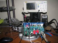
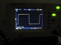
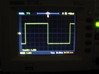
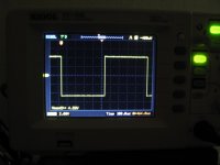
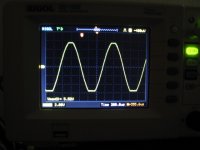
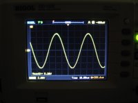
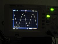
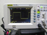
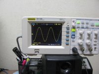
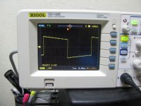
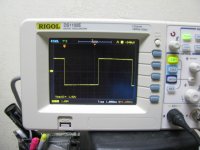
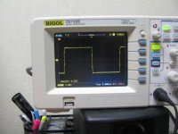
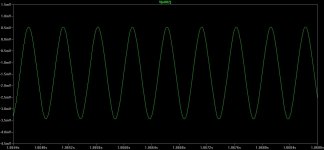
Here are the waveforms from some testing of this amp project, both for the first (gain) stage and the output stage powering headphones.
The first photo is the test setup. A function generator going into one channel and a scope on the output. The gain stage waveforms are taken off the input to the 1K attenuation resistor, which is the output of one channel's LME49990 gain chip. The output stage waveforms are taken off the amp output with a fairly sensitive 110dB/V set of test headphones (100mV for full volume, approximately).
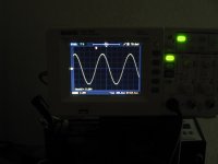
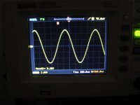
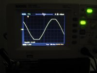
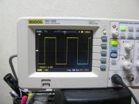
The next photos are checking for clipping behavior. I increased a sine wave's amplitude until one of the rails clipped at 1kHz, then ran it down to 10Hz and up to 20Khz to see how consistant everything is. The result: extremely consistent vs. frequency! Almost nil change in amplitude or clipping level from 10Hz to 20kHz.
The clipping first occurs at -5.6Vdc on the negative rail, because the gain stage will have a small amount of DC offset from the chip's input offset voltage, the 10K input resistor (times the op amp input bias current) and then increased by the closed loop gain of the stage. All of this is the same for RocketScientist's O2 amp, which is one of the reasons he included that coupling cap in the middle to isolate gain stage offset from the output stage. If the signal amplitude is run up further (as shown in one photo) until the positive rail clips, it is also at +5.6Vdc. So no lack of symmetry in the amp per se, just the normal DC offset.
One of the outcomes here is to verify where I have the clipping indicator reference voltage levels set. The blue LEDs set the clipping points at about 2V below (positive rail) or above (negative rail). The results here show that for +/-7Vdc rails the clipping is at 7Vdc - 5.6Vdc = 1.4Vdc below the rail, and with the +/-16Vdc rails the clipping in the photos is 16Vdc - 14.5Vdc = 1.5Vdc. So for either rail voltage the clipping indicator LED will light about 1/2 volt *before* clipping actually occurs, which is exactly what I want it to do, to be an alert that signal levels are getting too high before they actually hit clipping. So I'm probably going to keep the internal blue LEDs, just tone then down a bit by increasing the series resistor so it doesn't glow blue through the end panel cracks.
Photos:
1-8 are all done with the power supply rails set to +/-7Vdc
1. test setup.
2. 1kHz gain stage output, showing neg half clipping onset at -5.6Vdc
3. 10Hz gain stage output, showing neg half clipping onset at -5.6Vdc
4. 20kHz gain stage output, showing neg half clipping onset at -5.6Vdc
5. 1kHz gain stage output, amplitude increased until both rails clip at +/-5.6Vdc
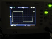
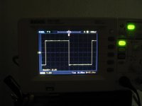
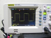
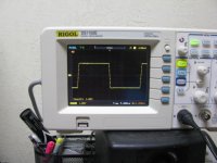
The next three have the amplitude backed down about a volt to stay away from clipping, to look at square wave waveshapes.
6. 1kHz gain stage output square wave.
7. 10Hz gain stage output square wave.
8. 20kHz gain stage output square wave.
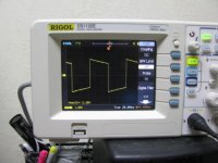
9 and 10 are done with the power supply rails set to +/-16Vdc
9. 1kHz gain stage output, amplitude run up to show clipping on both wave haves, clipping onset on both wave halves at 14.5Vdc
10. 10Hz gain stage output, clipping onset on both wave halves at 14.5Vdc
The first photo is the test setup. A function generator going into one channel and a scope on the output. The gain stage waveforms are taken off the input to the 1K attenuation resistor, which is the output of one channel's LME49990 gain chip. The output stage waveforms are taken off the amp output with a fairly sensitive 110dB/V set of test headphones (100mV for full volume, approximately).
The next photos are checking for clipping behavior. I increased a sine wave's amplitude until one of the rails clipped at 1kHz, then ran it down to 10Hz and up to 20Khz to see how consistant everything is. The result: extremely consistent vs. frequency! Almost nil change in amplitude or clipping level from 10Hz to 20kHz.
The clipping first occurs at -5.6Vdc on the negative rail, because the gain stage will have a small amount of DC offset from the chip's input offset voltage, the 10K input resistor (times the op amp input bias current) and then increased by the closed loop gain of the stage. All of this is the same for RocketScientist's O2 amp, which is one of the reasons he included that coupling cap in the middle to isolate gain stage offset from the output stage. If the signal amplitude is run up further (as shown in one photo) until the positive rail clips, it is also at +5.6Vdc. So no lack of symmetry in the amp per se, just the normal DC offset.
One of the outcomes here is to verify where I have the clipping indicator reference voltage levels set. The blue LEDs set the clipping points at about 2V below (positive rail) or above (negative rail). The results here show that for +/-7Vdc rails the clipping is at 7Vdc - 5.6Vdc = 1.4Vdc below the rail, and with the +/-16Vdc rails the clipping in the photos is 16Vdc - 14.5Vdc = 1.5Vdc. So for either rail voltage the clipping indicator LED will light about 1/2 volt *before* clipping actually occurs, which is exactly what I want it to do, to be an alert that signal levels are getting too high before they actually hit clipping. So I'm probably going to keep the internal blue LEDs, just tone then down a bit by increasing the series resistor so it doesn't glow blue through the end panel cracks.
Photos:
1-8 are all done with the power supply rails set to +/-7Vdc
1. test setup.
2. 1kHz gain stage output, showing neg half clipping onset at -5.6Vdc
3. 10Hz gain stage output, showing neg half clipping onset at -5.6Vdc
4. 20kHz gain stage output, showing neg half clipping onset at -5.6Vdc
5. 1kHz gain stage output, amplitude increased until both rails clip at +/-5.6Vdc
The next three have the amplitude backed down about a volt to stay away from clipping, to look at square wave waveshapes.
6. 1kHz gain stage output square wave.
7. 10Hz gain stage output square wave.
8. 20kHz gain stage output square wave.
9 and 10 are done with the power supply rails set to +/-16Vdc
9. 1kHz gain stage output, amplitude run up to show clipping on both wave haves, clipping onset on both wave halves at 14.5Vdc
10. 10Hz gain stage output, clipping onset on both wave halves at 14.5Vdc
Attachments
-
 IMG_1937.JPG192.9 KB · Views: 296
 -
 IMG_1938.JPG104.4 KB · Views: 279
 -
 IMG_1939.JPG118.5 KB · Views: 266
 -
 IMG_1947.JPG109.3 KB · Views: 70
 -
 IMG_1945.JPG112.9 KB · Views: 77
 -
 IMG_1944.JPG107.1 KB · Views: 70
 -
 IMG_1946.JPG112.9 KB · Views: 68
 -
 IMG_1942.JPG115.3 KB · Views: 256
 -
 IMG_1941.JPG120.2 KB · Views: 269
 -
 IMG_1948.JPG115.6 KB · Views: 59
Last edited:
...testing continued
I ran out of attachments. Here is part 2...
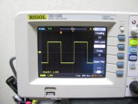
All using the +/-16Vdc power supply rail setting now. Amplitude backed down to about +/-12.6Vdc to avoid clipping to show the square wave shapes.
1. gain stage output square waves at 20kHz.
2. gain stage output square waves at 10Hz.
I ran out of attachments. Here is part 2...
All using the +/-16Vdc power supply rail setting now. Amplitude backed down to about +/-12.6Vdc to avoid clipping to show the square wave shapes.
1. gain stage output square waves at 20kHz.
2. gain stage output square waves at 10Hz.
Attachments
Here are some pictures of the parallel output stage under load. The test setup in the first photo is just a 15R and 43R 5W resistor sitting on a 2x4. These are all with the power supply rails set for the +/-7Vdc position to show the high current output capability of the amp for hard-to-drive headphones with low ohm loads and low sensitivity.
The first two scope shots show something the O2 headphone amp can't do. That is a 4Vpeak 1kHz square wave and sine wave into 15 ohms. For the sine wave that would be 4Vpk / 15R = 267mA(peak), or (4 * .707) / 15R = 188mA(rms). That is about twice the output current capability of the O2. The output chips were just slightly warm at that level since it is running on the +/-7Vdc power rail position.
The next 3 square wave shots are with the 43R resistor (my Shure SRH940s are 44R), +/-7Vdc rails, and a 2Vpeak wave. 1kHz, 10Hz, 100Hz, and 20kHz. The droop on the 10Hz square wave is the effect of the coupling cap, as expected, forming the high pass input filter with Fc = 1.12Hz.
The final 3 square wave shots are with the 15R resistor, +/-7Vdc rails, and a 2V peak wave. 20Khz, 10Hz, and 100Hz.
Attachments
-
 IMG_1958.JPG156.5 KB · Views: 71
 -
 IMG_1957.JPG150.7 KB · Views: 75
 -
 IMG_1956.JPG157.3 KB · Views: 527
 -
 IMG_1955.JPG146.5 KB · Views: 545
 -
 IMG_1964.JPG162.7 KB · Views: 552
 -
 IMG_1963.JPG157 KB · Views: 587
 -
 IMG_1954.JPG196.4 KB · Views: 594
 -
 IMG_1959.JPG156.8 KB · Views: 68
 -
 IMG_1960.JPG153.6 KB · Views: 76
 -
 IMG_1961.JPG145.9 KB · Views: 76
Last edited:
BOM changes
Here is a new BOM for this project with 3 changes.
In the scope shots I posted above of the 20kHz square wave the leading edge is a bit more rounded than I was expecting, indicating the stage was a bit overcompensated. I've backed the 220pF cap from the O2 amp down to 150pF and that fixed the issue. Scope shots below are before (220pF) and after (150pF).
Then over the weekend I had been listening to the amp for about an hour on the +/-7Vdc rail setting when C51 suddenly shorts out and goes up in a puff of smoke. That was a 22uF 20Vdc organic polymer capacitor running at just 7Vdc. Clearly a defective part, but regardless I'm switching those to 100uF 25Vdc low Z aluminum electrolytics - same size and lead spacing as the old cap. I'm leaving the 390uF 25V organic poly caps in for now given the extra 5 volts of rating on those. I've read that the failure mode on these new organic polymers is to short, just like the old tantalums, and sure enough it did. I always double the voltage rating on tantalums for that reason, along with their significant termperature derating curve. That wasn't an option for the organic poly's since their available voltage ratings are so low.
And R22 and R23 needed to be corrected on the BOM. I had changed those from SMD to low current noise through-hole.
Here is a new BOM for this project with 3 changes.
In the scope shots I posted above of the 20kHz square wave the leading edge is a bit more rounded than I was expecting, indicating the stage was a bit overcompensated. I've backed the 220pF cap from the O2 amp down to 150pF and that fixed the issue. Scope shots below are before (220pF) and after (150pF).
Then over the weekend I had been listening to the amp for about an hour on the +/-7Vdc rail setting when C51 suddenly shorts out and goes up in a puff of smoke.
That was a 22uF 20Vdc organic polymer capacitor running at just 7Vdc. Clearly a defective part, but regardless I'm switching those to 100uF 25Vdc low Z aluminum electrolytics - same size and lead spacing as the old cap. I'm leaving the 390uF 25V organic poly caps in for now given the extra 5 volts of rating on those. I've read that the failure mode on these new organic polymers is to short, just like the old tantalums, and sure enough it did. I always double the voltage rating on tantalums for that reason, along with their significant termperature derating curve. That wasn't an option for the organic poly's since their available voltage ratings are so low.And R22 and R23 needed to be corrected on the BOM. I had changed those from SMD to low current noise through-hole.
Attachments

Last edited:
Problem with your ODA BOM
When I download your BOM for the ODA project, all is well. But when I use Adobe Reader to display it, the BOM is to small to print. The size is set for 74% or so at
the start. I must blow up the BOM to at least 200% or 400% to read it. I have tried
various methods to print the larger size but have had no luck. Any ideas about to
obtain the larger print out of the BOM? Take care and I can't wait to build this
unit. Keep up the great work.
Here is a new BOM with the printing issues fixed. It will print out in landscape mode now (sideways). 12 pages all total (3 columns of 4 pages) including the part numbers for Mouser, Digikey, Farnell, Allied, Newark, Jameco, and RS Components and the notes. Please let me know about any BOM problems! I've double checked the Mouser and Digikey part numbers, but for the other providers be sure to double check the part vs. the description in case something got changed in an edit.
Attachments
Last edited:
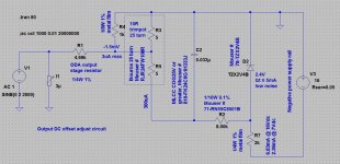
DC offset fixed passive reduction circuit
Here is something kind of interesting. From the table of per-output-chip DC offset numbers I posted a few posts back it appears that the NJM4556A output chips have a rather consistent DC offset. All around +1.5mVdc, plus or minus a few hundred microvolts.
So rather than a DC servo, it hit me that a fixed passive DC offset correction might work well. In other words return the input bias ground return resistor on the output stage to -1.5mVdc rather than ground to cancel out the combined amp DC output offset of +1.5mV. The results are below. All in all it seems to work extremely well and, most importantly, seems to be fairly stable over time. Unfortunately there is no space on the PC board to add the circuit but this might be a good addition to a top-slot accessory board at some point in the future.
The circuit is below. Just a 10 ohm precision 25 turn trimmer pot and series resistor being fed from a 2.5Vdc zener or precision voltage reference through a noise filter. There are a few advantages of the fixed circuit over a servo:
* No oscillation, either high frequency or subsonic. Since there is no (servo) feedback loop there are no loop oscillation problems.
* No virtual ground through an active class AB output stage. This circuit is essentially just 5 ohms to ground in series with the 4.99K input bias ground return resistor. If a OPA627, etc, is used in a DC servo loop there is the chance that the AC signal going in the reverse direction toward the chip's output could force the chip's output stage through the class AB transition region, potentially adding distortion. In other words, the DC servo chip's output essentiially is forming the dreaded virtual ground with the AC signal being returned to it. This is even more likely since the DC correction voltage being produced is just 1.5mV while the reverse direction AC signal (5R in series with 4.99k) can be up to 10mV or so with a full 10Vrms signal swing in the amp.
* (essentially) no frequency sensitive components. The corner frequency of the zener filter is high enough to be out of the way with the listed 0.033uF capacitor. An active precision DC servo chip may otherwise require an output T filter to start shunting the reverse AC signal to ground at 1kHz or so.
There is one hiccup with the circuit. The DC output offset voltage of the NJM4556A chips is around 1.45mV with +/-7Vdc power rails, but around 1.65mV Vdc with the +/-16Vdc rails. In other words, pushing the power rail voltage selector switch causes a 200 microvolt shift in overall DC output offset. From the photos below, the circuit works so well that either offset can be reduced to around 20uV. So one rail setting or the other can be nulled out, which will leave the other at around 400uV, which is still just 400uV / 1.45mV = 30% of the uncorrected DC offset in the "higher" position. The other way, which I've tested, is set the +/-7Vdc rail position for +200uV offset, which then cause the +/-16Vdc rail position to be -200uV. Either one is just 200uV / 1.5mV = 14% of the uncorrected value.
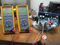
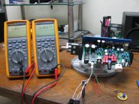
The first photo shows the test setup with the DC offset readings of the amp output on the two channels. The round circuit board is the implemented circuit but unhooked (red wire is output) at this point. 1.46mV and 1.63mV, again rather close and both the same polarity.
The next photo shows the circuit wired into one channel. The next photo shows the new DC offset on that channel. I was able to adjust the trim pot for just -4uV (microvolts!) of DC offset. The setting at this point is with the circuit only having been on about 5 minutes since power-on.
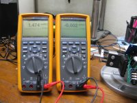
The last photo is the good stuff. This is 30 minutes of music playing later to warm up the parts, looking for the amount of thermal drift at this point. Essentially unchanged at -2uV. With the unit in the case where things would get a lot warmer inside I would expect more thermal drift than this, but still pretty darn good.
I didn't take a photo of the case where the +/-7Vdc rails were adjusted for -186uV of output DC offset, but the result in the +/-16Vdc rail position was around +195uV.
Here is something kind of interesting. From the table of per-output-chip DC offset numbers I posted a few posts back it appears that the NJM4556A output chips have a rather consistent DC offset. All around +1.5mVdc, plus or minus a few hundred microvolts.
So rather than a DC servo, it hit me that a fixed passive DC offset correction might work well. In other words return the input bias ground return resistor on the output stage to -1.5mVdc rather than ground to cancel out the combined amp DC output offset of +1.5mV. The results are below. All in all it seems to work extremely well and, most importantly, seems to be fairly stable over time. Unfortunately there is no space on the PC board to add the circuit but this might be a good addition to a top-slot accessory board at some point in the future.
The circuit is below. Just a 10 ohm precision 25 turn trimmer pot and series resistor being fed from a 2.5Vdc zener or precision voltage reference through a noise filter. There are a few advantages of the fixed circuit over a servo:
* No oscillation, either high frequency or subsonic. Since there is no (servo) feedback loop there are no loop oscillation problems.
* No virtual ground through an active class AB output stage. This circuit is essentially just 5 ohms to ground in series with the 4.99K input bias ground return resistor. If a OPA627, etc, is used in a DC servo loop there is the chance that the AC signal going in the reverse direction toward the chip's output could force the chip's output stage through the class AB transition region, potentially adding distortion. In other words, the DC servo chip's output essentiially is forming the dreaded virtual ground with the AC signal being returned to it. This is even more likely since the DC correction voltage being produced is just 1.5mV while the reverse direction AC signal (5R in series with 4.99k) can be up to 10mV or so with a full 10Vrms signal swing in the amp.
* (essentially) no frequency sensitive components. The corner frequency of the zener filter is high enough to be out of the way with the listed 0.033uF capacitor. An active precision DC servo chip may otherwise require an output T filter to start shunting the reverse AC signal to ground at 1kHz or so.
There is one hiccup with the circuit. The DC output offset voltage of the NJM4556A chips is around 1.45mV with +/-7Vdc power rails, but around 1.65mV Vdc with the +/-16Vdc rails. In other words, pushing the power rail voltage selector switch causes a 200 microvolt shift in overall DC output offset. From the photos below, the circuit works so well that either offset can be reduced to around 20uV. So one rail setting or the other can be nulled out, which will leave the other at around 400uV, which is still just 400uV / 1.45mV = 30% of the uncorrected DC offset in the "higher" position. The other way, which I've tested, is set the +/-7Vdc rail position for +200uV offset, which then cause the +/-16Vdc rail position to be -200uV. Either one is just 200uV / 1.5mV = 14% of the uncorrected value.
The first photo shows the test setup with the DC offset readings of the amp output on the two channels. The round circuit board is the implemented circuit but unhooked (red wire is output) at this point. 1.46mV and 1.63mV, again rather close and both the same polarity.
The next photo shows the circuit wired into one channel. The next photo shows the new DC offset on that channel. I was able to adjust the trim pot for just -4uV (microvolts!) of DC offset. The setting at this point is with the circuit only having been on about 5 minutes since power-on.
The last photo is the good stuff.
This is 30 minutes of music playing later to warm up the parts, looking for the amount of thermal drift at this point. Essentially unchanged at -2uV. With the unit in the case where things would get a lot warmer inside I would expect more thermal drift than this, but still pretty darn good.I didn't take a photo of the case where the +/-7Vdc rails were adjusted for -186uV of output DC offset, but the result in the +/-16Vdc rail position was around +195uV.
Attachments
Last edited:
Boards are ready to ship
I've tested the spare PC boards for this project enough now that I'm comfortable with shipping them out to those who expressed interest, if still interested. Please follow up in this thread in the Vendor's forum
http://www.diyaudio.com/forums/vendors-bazaar/237226-parallel-njm4556al-two-stage-amp.html
I've tested the spare PC boards for this project enough now that I'm comfortable with shipping them out to those who expressed interest, if still interested.
Please follow up in this thread in the Vendor's forumhttp://www.diyaudio.com/forums/vendors-bazaar/237226-parallel-njm4556al-two-stage-amp.html
Last edited:
I was really excited at first when I found this thread (and it's always great when people have new ideas/designs to contribute), but I can't help being a bit disappointed by what feels like a "throw money at problems that aren't even problems" approach .
-Have you tested cheaper opamps than the 627 in your gain stage? If so, are there any good drop-in replacements that would work with your board?
-Why do you need so many of the 4.7u Wima decoupling caps? With the capacitance you have there, the 3dB point of the RC filter seems to be at 1.2Hz. If you just put in one 4.7u each, the 3dB point is still at 6.8dB, which still seems fine.
-Is there any actual benefit to the 0.1% resistors over buying 10 times as many 1% parts and matching them with a good DMM? In other words, do any of the resistor positions depend on being a really accurate absolute value?
.-Have you tested cheaper opamps than the 627 in your gain stage? If so, are there any good drop-in replacements that would work with your board?
-Why do you need so many of the 4.7u Wima decoupling caps? With the capacitance you have there, the 3dB point of the RC filter seems to be at 1.2Hz. If you just put in one 4.7u each, the 3dB point is still at 6.8dB, which still seems fine.
-Is there any actual benefit to the 0.1% resistors over buying 10 times as many 1% parts and matching them with a good DMM? In other words, do any of the resistor positions depend on being a really accurate absolute value?
Last edited:
dfy - good questions!
The gain stage chip(s) are two of the LME49990's in the current design, for exactly that reason. The LME4990 is just $2.60 at Mouser these days vs. $28 for the high grade OPA627, with better audio/AC specs on the LME49990.
I had started out at the first of this thread with the OPA627 in a loop around the NJM4556A buffers but dropped that when I discovered intermittent 80kHz oscillations. I switched over to the "O2 amp" design with a gain stage and output stage separated with the coupling caps and using the LME49990s for the gain stage.
However it would still work to use a FET input SOIC8 op amp (OPA627, OPA1641) in place of the LME49990 if someone preferred. Sergey888 posted about preferring FET input amps a few posts back.
On the coupling caps, you are quite right that using fewer and accepting a slightly higher corner frequency is a great way to save some $$ on the build. I even have that in the current build instructions (I'll have those posted this weekend). Just one or two caps on each channel could be soldering in initially, then more added as budget permits.
Or not added at all. I wanted to keep the corner frequency at least the same as the 1.8Hz in the O2 and preferably a bit lower so it could be said to be "improved" since I know that having coupling caps would worry some folks. But as RocketScientist pointed out and measured, a corner of 1.8Hz is just not likely to make an audible difference in actual practice. And I fully agree with you, a corner of 6.8Hz will also probably not be audible, especially since a lot of headphones drop off significantly down that low. So there is a lot of leeway there to save some money by populating few caps and accepting slightly less bass response.
Also keep in mind (this is also in the build instructions) that instead of the 6 x 4.7uF along with the 1K attenuation resistor, 1K pot, and 4.99K output ground return resistor it could be built up like the O2 with no attenuation resistor (shorted), a 10K pot, a 40.2K output ground return resistor, and one 4.7uF cap on each channel. That is still a lower 3dB point than the O2 with its 2.2uF caps. In the build instructions I go through selecting attenuation resistor (if any), pot choice (1K, 5K, 10K), ground return resistor choice, and cap choice and how they interact. For example:
* 1K atten resistor + 1K pot + 6 (or few as above) 4.7uF caps + 4.99K gnd return
* no atten resistor + 1K pot + 6 (or few as above) 4.7uF caps + 4.99K gnd return
* 5K atten resistor + 5K pot + 2 4.7uF cap + 24K gnd return
* no atten resistor + 5K pot + 2 4.7uF caps + 24K gnd return
* 10K atten resistor + 10K pot + 1 4.7uF caps + 40.2K gnd return
* no atten resistor + 10K pot + 1 4.7uF caps + 40.2K gnd return (like the O2 amp)
The smaller resistance value pots will generate less Johnson/thermal noise. But I'll admit that I have not gone back and tried substituting the 10K pot + 4.7uF + 40.2k resistor combo and listened on high gain for noise. I've built mine up with the 1k pots which have been just completely background noise/hiss free in my listening. However, to be objective, what really needs to be done here is an AP or dScope measurement of noise floor which I can't unfortunately do. All I can say if from the math, the lower value pot will generate less noise.
And on the 0.1% resistors, that was a byproduct of wanting to use thin film SMD or thick film for lower noise. In Mouser's selections it seems that 0.1% is the most common and available for 1206 thin film while 1% is the standard for 1206 thick film. I actually did go through the design a couple of times looking for resistors that were not in the signal path that could be switched to the cheaper types That resulted in the handful of through-hole 1% metal films and a couple of 1206 SMD thin films in the relay circuit, and clipping detect circuit. The two Q reduction resistors in series with the CLC filter inductors in the power circuit are thick film by necessity, given the power rating required.
Another issue for 0.1%-ers is matching in the gain stage. I wanted some fairly close gain matching between channels. The pot is not that close though, typically 20% for any of the 9mm Bourns or Alps pots, so if anyone wants to really do some close matching they can measure their pot's tracking between sections with a DMM then adjust the gain resistors (the 1.5K feedback would hit all the gain positions) accordingly on one channel to match, up or down.
In general I've allowed for a lot on individual customization with this amp and I've written the build instructions up like that. What would you expect from someone who made a huge modification thread on the O2 amp? Fewer output NJM4556ALs could be used if high current isn't needed, the LT voltage regulators and associated parts could be left out and bypassed if someone wanted, etc. All of those customizations would cut some $$ off the build, traded for for some performnce parameters.
The gain stage chip(s) are two of the LME49990's in the current design, for exactly that reason. The LME4990 is just $2.60 at Mouser these days vs. $28 for the high grade OPA627, with better audio/AC specs on the LME49990.
I had started out at the first of this thread with the OPA627 in a loop around the NJM4556A buffers but dropped that when I discovered intermittent 80kHz oscillations. I switched over to the "O2 amp" design with a gain stage and output stage separated with the coupling caps and using the LME49990s for the gain stage.
However it would still work to use a FET input SOIC8 op amp (OPA627, OPA1641) in place of the LME49990 if someone preferred. Sergey888 posted about preferring FET input amps a few posts back.
On the coupling caps, you are quite right that using fewer and accepting a slightly higher corner frequency is a great way to save some $$ on the build. I even have that in the current build instructions (I'll have those posted this weekend). Just one or two caps on each channel could be soldering in initially, then more added as budget permits.
Or not added at all. I wanted to keep the corner frequency at least the same as the 1.8Hz in the O2 and preferably a bit lower so it could be said to be "improved" since I know that having coupling caps would worry some folks. But as RocketScientist pointed out and measured, a corner of 1.8Hz is just not likely to make an audible difference in actual practice. And I fully agree with you, a corner of 6.8Hz will also probably not be audible, especially since a lot of headphones drop off significantly down that low. So there is a lot of leeway there to save some money by populating few caps and accepting slightly less bass response.
Also keep in mind (this is also in the build instructions) that instead of the 6 x 4.7uF along with the 1K attenuation resistor, 1K pot, and 4.99K output ground return resistor it could be built up like the O2 with no attenuation resistor (shorted), a 10K pot, a 40.2K output ground return resistor, and one 4.7uF cap on each channel. That is still a lower 3dB point than the O2 with its 2.2uF caps. In the build instructions I go through selecting attenuation resistor (if any), pot choice (1K, 5K, 10K), ground return resistor choice, and cap choice and how they interact. For example:
* 1K atten resistor + 1K pot + 6 (or few as above) 4.7uF caps + 4.99K gnd return
* no atten resistor + 1K pot + 6 (or few as above) 4.7uF caps + 4.99K gnd return
* 5K atten resistor + 5K pot + 2 4.7uF cap + 24K gnd return
* no atten resistor + 5K pot + 2 4.7uF caps + 24K gnd return
* 10K atten resistor + 10K pot + 1 4.7uF caps + 40.2K gnd return
* no atten resistor + 10K pot + 1 4.7uF caps + 40.2K gnd return (like the O2 amp)
The smaller resistance value pots will generate less Johnson/thermal noise. But I'll admit that I have not gone back and tried substituting the 10K pot + 4.7uF + 40.2k resistor combo and listened on high gain for noise. I've built mine up with the 1k pots which have been just completely background noise/hiss free in my listening. However, to be objective, what really needs to be done here is an AP or dScope measurement of noise floor which I can't unfortunately do. All I can say if from the math, the lower value pot will generate less noise.
And on the 0.1% resistors, that was a byproduct of wanting to use thin film SMD or thick film for lower noise. In Mouser's selections it seems that 0.1% is the most common and available for 1206 thin film while 1% is the standard for 1206 thick film. I actually did go through the design a couple of times looking for resistors that were not in the signal path that could be switched to the cheaper types That resulted in the handful of through-hole 1% metal films and a couple of 1206 SMD thin films in the relay circuit, and clipping detect circuit. The two Q reduction resistors in series with the CLC filter inductors in the power circuit are thick film by necessity, given the power rating required.
Another issue for 0.1%-ers is matching in the gain stage. I wanted some fairly close gain matching between channels. The pot is not that close though, typically 20% for any of the 9mm Bourns or Alps pots, so if anyone wants to really do some close matching they can measure their pot's tracking between sections with a DMM then adjust the gain resistors (the 1.5K feedback would hit all the gain positions) accordingly on one channel to match, up or down.
In general I've allowed for a lot on individual customization with this amp and I've written the build instructions up like that. What would you expect from someone who made a huge modification thread on the O2 amp?
Fewer output NJM4556ALs could be used if high current isn't needed, the LT voltage regulators and associated parts could be left out and bypassed if someone wanted, etc. All of those customizations would cut some $$ off the build, traded for for some performnce parameters.- Home
- Amplifiers
- Headphone Systems
- A version of an O2 Desktop Amp (ODA)