John-
Yeah his dissapoearing is really the hangnail. This ODA project is a direct result.
From the various posts here and on his blog a lot of people were waiting for the ODA design he mentioned many times but never produced. I was too! Then he dropped off the radar. I waited for 9 months or so after he dissappeared to work on this version, once it seamed clear the official ODA would never happen.
I do agree that his big point was that performance did not degrade. One thing he certainly made crystal clear in all his writings is he was not in it for profit himself. Nothing would make me happier than if RS would suddenly re-appear and be willing to go through the ODA design here and modify it to his liking and specs.") We all finally would get our (official) ODA.
We all finally would get our (official) ODA.
From my standpoint, until I hear differently from RS / NwAvGuy, I'm going on the read of the license that home, personal, DIY is fine for derivitive works but commercial sale is not.
I do see one change I'm going to make. I just re-read what license wording have on the board. I had "GNU" on the brain and put GNU public license wording on the PCB, forgetting that he had used Creative Commons. I'll change that to specifically state it is NwAvGuy's original O2 Creative Commons license that applies, which was my intent, to prohibit commercial sale without his OK.
Hey thank you for bringing this whole issue up! It did need to be addressed. Anyone who does measurements on this ODA version, if that ever happens, needs to be fully aware of NwAvGuy's license terms.
Yeah his dissapoearing is really the hangnail. This ODA project is a direct result.
From the various posts here and on his blog a lot of people were waiting for the ODA design he mentioned many times but never produced. I was too! Then he dropped off the radar. I waited for 9 months or so after he dissappeared to work on this version, once it seamed clear the official ODA would never happen.
I do agree that his big point was that performance did not degrade. One thing he certainly made crystal clear in all his writings is he was not in it for profit himself. Nothing would make me happier than if RS would suddenly re-appear and be willing to go through the ODA design here and modify it to his liking and specs.
We all finally would get our (official) ODA.From my standpoint, until I hear differently from RS / NwAvGuy, I'm going on the read of the license that home, personal, DIY is fine for derivitive works but commercial sale is not.
I do see one change I'm going to make. I just re-read what license wording have on the board. I had "GNU" on the brain and put GNU public license wording on the PCB, forgetting that he had used Creative Commons. I'll change that to specifically state it is NwAvGuy's original O2 Creative Commons license that applies, which was my intent, to prohibit commercial sale without his OK.
Hey thank you for bringing this whole issue up! It did need to be addressed. Anyone who does measurements on this ODA version, if that ever happens, needs to be fully aware of NwAvGuy's license terms.
Last edited:
Yeah, I have been waiting on the ODA since it was first mentioned on Nwavguy's
blog. I am a big fan of what he has done, but I think we have done our due diligence on waiting for him to return. Agdr has stated that he wants to see his version of the ODA to measure as well or better than the O2. I don't see a problem here.
blog. I am a big fan of what he has done, but I think we have done our due diligence on waiting for him to return. Agdr has stated that he wants to see his version of the ODA to measure as well or better than the O2. I don't see a problem here.
V1.2 updated Gerbers, layout, schematic
As per the license discussion, here is a revised layout with the license wording on the PC board changed to reflect NwAvGuy's Creative Commons license.
I've made a few more upgrades. I realized that 5 of the 4.7uF coupling capacitors per channel are adequate rather than 6, chopping $10 off the cost. The corner frequency of the O2's 2.2uF + 40.2k pair is around 1.8Hz. With the 6 4.7uF caps and 4.99k the ODA previously was around 1.12Hz. Now with 5 caps the corner frequency is around 1.3Hz, still better than the O2.
And... getting rid of those caps freed up some PC board space to make another attempt at adding back in a linearization loop around each channel's paralleled buffers. Occured to me a couple of days ago that although the LME49990 is apparently way to fast to be using in a loop with the slow NJM4556AL buffers, the NJM2068 (the gain chip in the O2) is a lot more in the ballpark and should work. The unity gain bandwidth of the NJM2068 is 27Mhz vs. 110Mhz for the LME49990, vs just 8Mhz for the buffers. Still faster than buffers, but at least a fair shot at keeping the NJM2068 stable.
Plus, the best part, looking at the gain/phase curve the NJM2068 starts out at 0 degrees, going down to -90 (90 degrees lag) at unity gain. Recall from past posting that the NJM4556A has a 30 degree lag which starts dropping rapidly after the audio band. Together the loop should have a fairly large phase margin. Enough that I wouldn't be worried about the various headphone capacitive loads that could be attached. TI still hasn't come up with the gain/phase plot for the LME49990. The OPA627 that I tried for the loop at the start of this thread and eventually oscillated at 70K started out with the fairly large 90 degree phase lag, which together with the NJM4556A's lag resulted in no phase margin.
RocketScientist / NwAvGuy wrote that he measured the NJM2068 at having lower distortion than the NJM4556A and that the distortion numbers of the NJM4556A are theerfore the limiting factor in the O2. So if the loop here works properly, there is at least the possibility of reduced output stage distortion vs. the O2. I've laid it out so that the NJM2068 loops on the output don't have to be used. The parts can be left unpopulated and 1206 0R jumper resistors soldered in to bridge input to output, in which case the design reverts to the previous V1.1 without the output stage feedback loop.
I'm going to pull a RocketScientist / NwAvGuy at this point and disappear myself. John has some very good points about the licensing questions with the ODA. I'm not going to sink any more time into it. But these Gerbers should be fully functional if anyone should want to give it a try, although for home use and not commercial sale.
As per the license discussion, here is a revised layout with the license wording on the PC board changed to reflect NwAvGuy's Creative Commons license.
I've made a few more upgrades.
I realized that 5 of the 4.7uF coupling capacitors per channel are adequate rather than 6, chopping $10 off the cost. The corner frequency of the O2's 2.2uF + 40.2k pair is around 1.8Hz. With the 6 4.7uF caps and 4.99k the ODA previously was around 1.12Hz. Now with 5 caps the corner frequency is around 1.3Hz, still better than the O2.And... getting rid of those caps freed up some PC board space to make another attempt at adding back in a linearization loop around each channel's paralleled buffers. Occured to me a couple of days ago that although the LME49990 is apparently way to fast to be using in a loop with the slow NJM4556AL buffers, the NJM2068 (the gain chip in the O2) is a lot more in the ballpark and should work. The unity gain bandwidth of the NJM2068 is 27Mhz vs. 110Mhz for the LME49990, vs just 8Mhz for the buffers. Still faster than buffers, but at least a fair shot at keeping the NJM2068 stable.
Plus, the best part, looking at the gain/phase curve the NJM2068 starts out at 0 degrees, going down to -90 (90 degrees lag) at unity gain. Recall from past posting that the NJM4556A has a 30 degree lag which starts dropping rapidly after the audio band. Together the loop should have a fairly large phase margin. Enough that I wouldn't be worried about the various headphone capacitive loads that could be attached. TI still hasn't come up with the gain/phase plot for the LME49990. The OPA627 that I tried for the loop at the start of this thread and eventually oscillated at 70K started out with the fairly large 90 degree phase lag, which together with the NJM4556A's lag resulted in no phase margin.
RocketScientist / NwAvGuy wrote that he measured the NJM2068 at having lower distortion than the NJM4556A and that the distortion numbers of the NJM4556A are theerfore the limiting factor in the O2. So if the loop here works properly, there is at least the possibility of reduced output stage distortion vs. the O2. I've laid it out so that the NJM2068 loops on the output don't have to be used. The parts can be left unpopulated and 1206 0R jumper resistors soldered in to bridge input to output, in which case the design reverts to the previous V1.1 without the output stage feedback loop.
I'm going to pull a RocketScientist / NwAvGuy at this point and disappear myself.
John has some very good points about the licensing questions with the ODA. I'm not going to sink any more time into it. But these Gerbers should be fully functional if anyone should want to give it a try, although for home use and not commercial sale.Attachments
Last edited:
I've had some email. I'm not leaving the forum and the audio hobby world, just this project until such time as the license issues John mentioned become clearer. I've run a couple of tech businesses over the years and I take contracts and intellectual property seriously, as I'm sure John does with JDS.
For what it is worth, after some discussions this week, I don't have any answers but I do have a bunch of interesting pointers for anybody else looking into the O2 licensing problem.
As for the Creative Commons licenses, they claim to be written to not override the normal exclusions of Fair Use and Public Domain / Prior Art. In the CC-BY-ND license that RocketScientist / NwAvGuy used for the O2 amp:
Creative Commons — Attribution-NoDerivs 3.0 Unported — CC BY-ND 3.0
scroll down to “with the understanding that” and the bullet points about “public domain” and “Fair Use”
Fair Use is the doctrine that says a copyright holder cannot dictate how a person uses the copyright “for their enjoyment”, along with commentary and criticism of the work. There apparently has been a pretty good body of case law built up over the years:
Fair use - Wikipedia, the free encyclopedia
As it applies here, my best understanding of it all is still that non-commercial DIY work would constitute Fair Use. Internet postings of non-commercial DIY modifications may be a first amendment / free speech issue, same as publishing a how-to book on a subject.
Public domain and/or prior art relates to works already in the public domain. In the case of the O2, it is full of what are likely public domain works-
Welcome to the Public Domain :: Copyright Overview by Rich Stim :: Stanford Copyright and Fair Use Center
which may apply to the O2. But for that type of copyright to hold up in court, it may need to be extremely specific and narrow in scope, such as a portable headphone amp with 2 batteries (maybe even as specific as 2 NiMH 9V batteries), a power management circuit, with a certain circuit arrangement, etc. Otherwise, if applied broadly, such a copyright would apply to any portable headphone amp with batteries and two amp stages.
Which then goes to the issue of derivative works. Derivative works are their own chunk of copyright law:
Derivative work - Wikipedia, the free encyclopedia
An issue that comes up is "when is a work different enough so as not to be a derivative, but rather a unique work?" In the case of the amp here a few points of difference from the O2 amp are:
* No batteries, no charging circuit, not portable
* No power management circuit
* Different chips in the gain stage, two singles vs. one dual
* Different regulator circuit with different chips and 2 voltages, both different
* Different case and PCB form factor
* Unique layout, not a copy of the O2 layout
* Clipping indicator circuit
* Relay protection circuit
* SMD along with through hole parts, both sides of the PCB rather than one
* SIPs instead of DIPs for the output stage
but similar things
* pot in the middle with coupling caps
* parallel buffers, although more of them, using the NJM4556A chips
* 3.5mm input and output jacks, although other too
I don't have an answer here. I wish I did! But it certainly is a good question. Is it a derivative work or a new work?
And finally there is the issue about NwAvGuy disappearing, which turns out to be more of a can of worms than I realized. The concept of an "Orphaned Work" would seem to apply:
Orphan works - Wikipedia, the free encyclopedia
Orphan works in the United States - Wikipedia, the free encyclopedia
Apparently the law here is a mess after the Copyright Act of 1976 did away with the requirement to actually register a copyright with the PTO. So now there is no way for anyone to know if the original copyright holder or their representative is still around, much less how to contact them. Apparently various legislative solutions have been proposed since, but nothing passed or solved.
So yes, from my read of it, in the US right now it is apparently possible for an original copyright holder to suddenly show up after years of dissapearance and still own the copyright.
Interesting stuff!
What I may do is eventually break up the layout I already have here into "public domain pieces" as individual PCBs, like the power supply and gain stage, which would seem to get around the issue of copyrighting a specific collection of public domain pieces as an complete work.
I'm not leaving the forum and the audio hobby world, just this project until such time as the license issues John mentioned become clearer. I've run a couple of tech businesses over the years and I take contracts and intellectual property seriously, as I'm sure John does with JDS.For what it is worth, after some discussions this week, I don't have any answers but I do have a bunch of interesting pointers for anybody else looking into the O2 licensing problem.
As for the Creative Commons licenses, they claim to be written to not override the normal exclusions of Fair Use and Public Domain / Prior Art. In the CC-BY-ND license that RocketScientist / NwAvGuy used for the O2 amp:
Creative Commons — Attribution-NoDerivs 3.0 Unported — CC BY-ND 3.0
scroll down to “with the understanding that” and the bullet points about “public domain” and “Fair Use”
Fair Use is the doctrine that says a copyright holder cannot dictate how a person uses the copyright “for their enjoyment”, along with commentary and criticism of the work. There apparently has been a pretty good body of case law built up over the years:
Fair use - Wikipedia, the free encyclopedia
As it applies here, my best understanding of it all is still that non-commercial DIY work would constitute Fair Use. Internet postings of non-commercial DIY modifications may be a first amendment / free speech issue, same as publishing a how-to book on a subject.
Public domain and/or prior art relates to works already in the public domain. In the case of the O2, it is full of what are likely public domain works-
- Half wave power supply
- Voltage doubler
- Regulators using off the shelf chips
- Non-inverting op-amp and unity gain buffer op amp stages
- Use of NJM4556A in a headphone amp (the Grado RA1)
- Input RF filter (out of one of Doug Self's books)
- Parallel op amps (the Meier parallel amp)
- Trickle NiMH battery charging
- The power management circuit
- Pot and coupling cap in the middle
Welcome to the Public Domain :: Copyright Overview by Rich Stim :: Stanford Copyright and Fair Use Center
which may apply to the O2. But for that type of copyright to hold up in court, it may need to be extremely specific and narrow in scope, such as a portable headphone amp with 2 batteries (maybe even as specific as 2 NiMH 9V batteries), a power management circuit, with a certain circuit arrangement, etc. Otherwise, if applied broadly, such a copyright would apply to any portable headphone amp with batteries and two amp stages.
Which then goes to the issue of derivative works. Derivative works are their own chunk of copyright law:
Derivative work - Wikipedia, the free encyclopedia
An issue that comes up is "when is a work different enough so as not to be a derivative, but rather a unique work?" In the case of the amp here a few points of difference from the O2 amp are:
* No batteries, no charging circuit, not portable
* No power management circuit
* Different chips in the gain stage, two singles vs. one dual
* Different regulator circuit with different chips and 2 voltages, both different
* Different case and PCB form factor
* Unique layout, not a copy of the O2 layout
* Clipping indicator circuit
* Relay protection circuit
* SMD along with through hole parts, both sides of the PCB rather than one
* SIPs instead of DIPs for the output stage
but similar things
* pot in the middle with coupling caps
* parallel buffers, although more of them, using the NJM4556A chips
* 3.5mm input and output jacks, although other too
I don't have an answer here. I wish I did! But it certainly is a good question. Is it a derivative work or a new work?
And finally there is the issue about NwAvGuy disappearing, which turns out to be more of a can of worms than I realized. The concept of an "Orphaned Work" would seem to apply:
Orphan works - Wikipedia, the free encyclopedia
Orphan works in the United States - Wikipedia, the free encyclopedia
Apparently the law here is a mess after the Copyright Act of 1976 did away with the requirement to actually register a copyright with the PTO. So now there is no way for anyone to know if the original copyright holder or their representative is still around, much less how to contact them. Apparently various legislative solutions have been proposed since, but nothing passed or solved.
So yes, from my read of it, in the US right now it is apparently possible for an original copyright holder to suddenly show up after years of dissapearance and still own the copyright.
Interesting stuff!
What I may do is eventually break up the layout I already have here into "public domain pieces" as individual PCBs, like the power supply and gain stage, which would seem to get around the issue of copyrighting a specific collection of public domain pieces as an complete work.
Last edited:
copyright only protects an exact copy of an expression - not the ideas/technology - only active, valid patents can in principle protect published circuits from being reused/reimplemented by others
even for a schematic copyright - only the exact, particular drawing can be subject to copyright - anyone can fire up their own favorite schematic entry tool and re-enter the exact same circuit - and freely publish it - protect their own drawing of it under copyright - but the topology, circuit ideas, methods, implementation, parts choices are not copyright-able
likewise copyright can protect the exact grahics image of a particular PCB layout of a circuit, or the Gerbers, even the PCB itself is considered an copyrigh-able graphic work - but anyone can redo the layout without facing restriction from copyright
Last edited:
Hey thanks for the feedback, jcx! Very helpful.
Yeah I've had some additonal PMs, emails, and discussions and the net result is that there apparently isn't a problem here. A "derivative" work apparently has to be vastly more similar than this amp. Someone has even pointed out that RS himself referred to the ODA as a separate project that he would produce at some point.
In fact, it may be the case that if I believe this amp isn't an O2 "derivative" then I should be leaving the mention of NwAvGuy off the board entirely. Still looking ito that one. That is unfortunate since I really respect his work and wanted to give credit were due! RS clearly was vastly better at this stuff than me with a lot more audio industry experience.
So apparently no problem after all. But thanks again to John for bringing it up! Needed to be discussed and would have come up eventually.
Back to the technology... if anyone etches the last set of Gerbers I posted, two things need to be done. First I've realized that the 0.51R CLC resistors really should be a higher wattage for longevity given the half wave charging spikes. I've changed those to 2512 2W SMD parts, but an easy fix on the board is leave the two surface mount 1206 SMD resistors off and just solder a through-hole axial 0.51R 2W between the two pins on the cap and inductor that the SMD traces went to for each resistor, right under the board. Plenty of space in the case for that. Or the two 0.51R resistor pads can simply be shorted. Those resistors are just a small tweak to lower the Q of the filter circuit to get rid of a tiny amount of overshoot.
Second the NJM2068 loop around the output buffers is likely not going to work, so leave that chip off and use the two 0R bypass resistors that I included on the layout to feed the output buffer chips directly from the coupling caps. I was able to reproduce the triangle wave oscillation that I saw with the LME49990 loop chips in an LT Spice simulation using the NJM2068 chips instead and the output buffers. I believe I know what is going on now. It is likely more related to slew rate, in having a faster slewing chip (the NJM2068) powering a slower slewing chip (NJM4556AL at only 3V/uS). The slow chip trying to keep up with the faster slewing chip produces the small-amplitude triangle waveform.
This one was a little tricky to figure out. The audio has a swing of up to 10V rms with the 17Vdc rails. So with a 3V/uS slew that would be about 3.2uS for 1/4 of the wave or a frequency of 78kHz for the full cycle. Still adequate for audio. But the problem is with much smaller amplitude swings (noise) which takes considerably less time even at 3V/uS, and can result in small amplitude, but fast frequency, triangle wave oscillation.
There really isn't a workable audio-capable chip with a slew less than 3V/uS to wrap around the NJM4556As that I can find, so the best solution is just not to go there with this design and leave the NJM2068 chips around the buffers out entirely. Just feed the buffers directly from the coupling caps, as in the O2 by using those 0R 1206 resistors.
Last edited:
...That is unfortunate since I really respect his work and wanted to give credit were due! RS clearly was vastly better at this stuff than me with a lot more audio industry experience.....
Exactly my thoughts!
Output balancing resistor measurements
I've attached an interesting set of measurements below. These are the DC output offset voltages at idle, with no input signal, for each half of each NJM4556AL output chip. One bank of 3 paralleled chips (6 outputs) has 1 ohm resistors, same as the O2, while the other bank has 3.32 ohm resistors.
With just two chip halves paralleled the O2 amp has an effective output resistance of 0.5R. With 6 chip halves paralleled and using 1R resistors the effective output impedance is around 0.17R. With the 3.32R resistors it goes back up to 0.55R, similar to the O2.
Smaller balancing resistors cause higher balancing currents to flow and increase chip power dissipation, but pull the various outputs closer together. The larger 3.32R resistors reduce the balancing current and allow the chip outputs to move closer to their natural idle state.
One of RS's theories was that the two halves of any given NJM4556A chip would be fairly well matched since they are on the same die, vs comparing halves of different chips. That seemed to be the case measuring the O2 with the 1R balancing resistors. But with the 3.32R resistors unbinding the outputs a bit it actually doesn't look like the case. For example, from the last entry, -83uV difference from the average on one chip half and +305uV on the other. Which means that going to multi-chip balancing in this amp, with 3 chips per channel, shouldn't produce much of a different result in terms of matching than with just one chip per channel in the O2. Just more current capability.
Going into these measurements I was not expecting the DC output offsets of the various chips to be so well matched. I was expecting things more on the order of around +4mV output on one chip and -2mV on the other to produce the 2mV average, resulting in large(r) balancing currents. Instead they are all positive voltages just a few tens or hundreds of uV away from each other.
The balancing currents involved are tiny - hundreds of uA - so neither 1R or 3.32R will heat up the chips much and subtract from the total chip 800mW dissipation capability, even at +/-17Vdc power rails. The chip quiescent current dissipates more than that. Either value would work. I've read a suggestion from a power op amp manufacturer in an app note to use balancing currents per chip (chip half in this case) of around 1% of the chip's output current capacity when paralleling chips. For the NJM4556AL that would be 70mA / 100 = 700uA. It looks like a balancing resistor value of around 0.5R would be closer to that, from the measured numbers here.
Attachments
Last edited:
One of RS's theories was that the two halves of any given NJM4556A chip would be fairly well matched since they are on the same die, vs comparing halves of different chips.
I was so surprised by his theory that I did some measurements on about 25 of these chips. Whereas most were fairly well matched that I reckon was because the offsets were fairly low anyway. I did find one chip with a big difference in offset between the two halves. Only one device is needed to invalidate a hypothesis.
Since then I found an article from TI which contradicts RS's theory. I put the link up on my blog - http://www.diyaudio.com/forums/blogs/abraxalito/753-whats-datasheet.html
abraxalito- thank you for the confirmation! I always worry that I've missed something in these test setups.
Well that is interesting. So it looks like 0.5R might be a better balancing resistor. Mouser doesn't have 0.5R metal film in 1/8W, but they do in the standard 6mm length 1/4W, which should fit just fine if "tombstoned" on end. The lead diameter of the bigger resistor is 0.64mm diameter and the board hole is 0.82mm, so all should still fit.
The output chips get warm at idle with no signal (and no oscillation showing up on a 100mHz scope), more so with the 17V rails, and I originally figured that was due to balancing currents. But no, it is just apparently due to the quiescent current of around 11mA per chip, from the data sheet. That would be 17Vdc * 2 rails * 11mA = 374mW, or roughly 47% of the chip's 800mW power dissipation rating taken up just with quiescent current dissipation.
I'm probably going to reduce the upper rail voltage from +/-17Vdc to +/-16Vdc. That will help with dissipation a bit. I've also been concerned about the +/-15Vdc maximum input of the NJM4556A's with supply rails over 15V, from the datasheet. I've been relying on the output swing of the gain stage LME49990s to not exceed that, from the datasheet numbers (around 2.5V below the rails maximum), but lowering the rails a volt would guarantee the parameter never gets exceeded.
Last edited:
Hey agdr, sweet project! Its clear you've put a lot of effort into it and I would love to hear it.
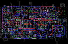
If I could make one suggestion, it would be to clean up your schematic in Eagle and split it up over multiple sheets. As it stands, its pretty hard to decipher everything that's going on.
Olin Lathrop has a great post on how to keep schematics tidy and legible.
Rules and guidelines for drawing good schematics - Electrical Engineering Stack Exchange
If I could make one suggestion, it would be to clean up your schematic in Eagle and split it up over multiple sheets. As it stands, its pretty hard to decipher everything that's going on.
Excellent suggestion! Thanks.
I didn't know Eagle could do that. I've only been using Eagle for about 6 months now, so definitely still in the learning mode. Its been a couple of decades since I last laid anything out.Hey I just adopted one of your design points. I had forgotten about that 300mW surface mount version of the NJM4556A until I saw it in your design. Earlier in the thread it was suggested to add a pre-amp output jack on the front. I've finally got onboard the train and decided that is a good idea. That NJM4556AM surface mount chip makes the perfect buffer for the pre-amp out! 300mw is perfectly adequate for just driving an RCA cable and line-level pre-amp inputs. Earlier in the thread I was thinking of taking pre-amp outs directly off of the gain stage LME49990 chip, but that would be a bad idea due to cable capacitance.
Attachments
Excellent suggestion! Thanks.
IMHO distortion & noise figures will be less with NE5532 instead of NJM4556AM.
Last edited:
agdr, glad to see this project. Regarding the CC license. One way to read it is that since your design is such as departure from the original design. it is no longer a derivative (in regard of copyright) and you don't need to worry about the original license.
But the wording of the CC license does seem to imply "any improvements" on the work. If this were the case, we would be still driving model Ts
But the wording of the CC license does seem to imply "any improvements" on the work. If this were the case, we would be still driving model Ts
IMHO distortion & noise figures will be less with NE5532 instead of NJM4556AM.
Yeah, I agree, I am already thinking that for the pre-amp out, passing along the low noise and distortion from the gain stage is important. That NE5532 or the LME49720 would fit in the same surface mount PCB footprint. Then just use an output series resistor to isolate the cable capacitance. That resistor shouldn't be a problem with the relatively high impedance line out rather and low impedance cans.
But the wording of the CC license does seem to imply "any improvements" on the work. If this were the case, we would be still driving model Ts
Very true!
That would have been the end of any innovation. The same goes for this amp. I fully expect that someone out there may eventually make their own version, and that is great. Discrete transistors could be used for the output stage and all sorts of other modifications.V 1.4 Gerbers, layout, circuit, BOM, changes
Here is the latest and hopefully last revision of this project. Gerber files, layout, circuit, BOM, and list of changes. Still coming are updated build instructions and Front Panel Express CAD files.
The change list has the details. The DC servo is gone, output balancing resistors changed to 0.5R, pre-amp jack and optional buffer/amp added, the 6th coupling cap on each channel is back for a Fc of 1.12Hz, upper power rail voltage switch choice is now +/-16Vdc isntead of +/-17Vdc, test points added for the pre-regulator voltages, and CLC resistors now 2512 size.
Feeding the pre-amp out jacks from the gain stage doesn't make any sense given that it can produce up to 10V of swing for the output stage and we need line level. Instead a twisted pair of wires from PCB holes provided can be used to hook it up in various ways:
* Connect to the input jacks for signal pass-through
* Run the input jacks through a new 1x buffer stage for pass-through with current buffer
* Same as above, but add a gain resistor for voltage gain. Default is 2.5x.
* And the option is still there to hook the pre-amp out to the out of the gain stage or even amp output, if needed.
The OPA2188 chip turned out to be useless for the DC servo in some testing I've done. I missed that the input offset current with the chip is so large that when multiplied by the servo resistors produces an offset of about the same size as what is being corrected. I tried an OPA627 instead and that did work well for the servo, dropping the DC offset to about 250mV. But the 80kHz oscillation from the start of this thread was back, due to the 90 + 60 degree lag leaving no phase margin in the loop. The new 0.5R balancing resistors further lower the output offset to about 1mV, so I'm dropping the DC servo entirely and calling that good. Still 3x lower output DC offset than the O2 amp.
Attachments
Last edited:
Procedure to obtain PCB's
I have not ordered PCB's before so I need help. Please direct me to your
source of PCB's in China. I need there WEB Address, etc.
I also need the procedure to use to submit your Gerber files to this company.
I assume it's something like the following:
(1) Go to the PCB's Vendors WEB Site
(2) Sign up for an account
(3) Download the Gerber files
(4) etc.
I need this procedure to be filled in, I'm guessing here. I assume you pay via
PayPal but I do not know. Help!!
I believe your design is SO different from the original Objective 2 design, that
I would give it a new name, version number (1.4), etc. Objective 2 was
portable, the ODA is not. Objective 2 uses batteries, the ODA does not.
Some of the basic theory tracks the Objective 2, but can you Copyright
Theory? I don't think so. Please do not give up on this project. I learn
so much from reading your posts. I'm sure the Objective 2 creators would
above. Take care.
I have not ordered PCB's before so I need help. Please direct me to your
source of PCB's in China. I need there WEB Address, etc.
There's no need to go to a major PCB shop for small projects.
Try OSHPark. Very fast, high quality, and much cheaper. We use them for prototypes. Their site should walk you through the basics.
I have not ordered PCB's before so I need help. Please direct me to your source of PCB's in China. I need there WEB Address, etc.
Well I may have some good news on the PC board end of things.
I just visited the various PCB vendor sites to make sure I was giving you up to date info, and I see that Seeed Studio now is offering 4 layer boards in the 10 x 20 size:
Fusion PCB Service - 4 Layers [PCB02281P] - $39.90 : Seeed Studio Bazaar, Boost ideas, extend the reach
My original intent with the desktop amp was to use a 4 layer board, but Itead Studio, the outfit I've been using, only had 4 layer up to 10 x 10. The last time I checked Seeed Studio they only offered 4 layer up to 10 x 10 so this may be something new.
So I'm going to probably order another run of boards from Seeed Studio and do it with 4 layer. Layer 2 will be a full ground plane single-point grounded (shielding and consistant impedance only, carrying no currents) and the 3rd layer used to get rid of most or all of the wire jumpers on the current board.
My main intent with the board run is to build one up and check the 4 layer design, but it looks like I get 10 boards for $120 plus $32 in DHL express costs, or about $15.20 a board. I want to keep 3 bare boards, but that leaves 6.
Assuming all works properly when I build the test board up, I'll go ahead and make the remaining 6 available at cost plus shipping if anyone is interested. Just send me a PM. I'll have to PM the moderators and find out what the appropriate forum is here for such thing for the subsequent follow-ups, group buy forum, vendors forum, etc. I'll even make a $1 donation to the forum out of my pocket for each board. Anyone interested in the remaining boards just PM me and I'll parcel the 6 out in order of requests received. 1 board maximum per person and anyone can decide to "opt out" along the way if they change their mind. I'll only collect money via paypal when it comes time to ship out. Shipping will be somewhat more expensive since I insist on using something with tracking and/or delivery confirmation. Here in the US postal service priority mail plus delivery confirmation would do the job, which is probably $7 or so. I'll find out. I'm going to have to do some work to add the 3rd and 4th layers so it may be a couple of weeks before I send an order out. Then once I get the boards back probably another week or so for me to build up one and test/verify it.mrsavage - if interested you can have first dibs on one of the extras at the $15.20 plus shipping cost so you don't have to buy a whole run of them.
No pressure though, go right ahead and do an order yourself if you want. Here are the details on the board houses. Good you asked, I've forgotten to post that information.I've been using Itead studio, which is here:
PCB prototyping
The "2 layer PCB larger than 10cm by 10cm" service is on the second page, page link at the bottom of the first page. Click "add to cart" on that "larger than 10x10" service and fill in the following parameters in the drop down boxes:
* PCB thickness = 1.6mm
* Surface Finish = HASL (hot air solder leveling)
* Etest = 100% (my understanding is there is no additional charge for this)
* PCB color = green (or any other color on the list for an additional $10 or so)
* PCB size = 10cm x 20cm (the amp is 80mm x 160mm = 8cm x 16cm)
The 10x20 size option adds $27 to the base service price of $38, for a total of $65 which will show up in the cart. That is for 5 boards. Then they offer DHL express for about $20, which is what I've been using (about 4 days ship time), or surface mail for $10 which could be a month or two ship time with no tracking. So all together $65 + $20 ship = around $85 for 5 boards, or about $17 per board.
It has only taken iTead about 8 calender days to get the boards done! This last time I submitted the design files late Sunday in the US, which is Monday AM in China, and on Friday of that same week received a ship notification email. Pretty impressive. DHL's tracking showed the boards picked up late Thursday of that week, in Hong Kong Friday, Cincinnati Saturday (US DHL hub) and to me Monday afternoon. DHL has their own in-house customs which avoids the typical 2-4 week "stall" in customs for postal mail from China.
How it works is that your shopping cart payment provides just an order number. Then you send them an email with that order number in the subject line and the Gerber files as an attachment (that exact zip file I posted). The email goes to pcb@iteadstudio.com. They then email a confirmation back. The subject line would be like: "order xxxxxxxxx (fill in your number) 8x16 green HASL1.6mm 5 pcs". They won't email again until the boards ship, and that email includes the DHL tracking number to view progress on DHL's site.
The Gerbers I posted were produced using a Eagle CAM processor job that iTead has posted on their site for use with Eagle 6.4. I haven't tried the files with other PC Board fab places like Seeed or OSH Park, which is another reason I'm kind of eager to try it with Seeed.
The processors I've heard about so far for small batches like this are iTead Studio, Seeed Studio, and like John says OSH Park. From what I read on the net most people think that iTead Studio and Seeed Studio are using the same wholesale board fabricator in China. I found a fantastic statistical analysis someone had done of all 3 services but I can't find that link now. The bottom line was that for just a few boards iTead was the cheapest with Seeed Studio close behind, but for slightly larger orders OSH Park won out. He also reviewed Sparkfun's board service and that came out most expensive of the bunch. I've seen posts saying what John is saying, that the quality of the OSH Park stuff is excellent.
Last edited:
- Home
- Amplifiers
- Headphone Systems
- A version of an O2 Desktop Amp (ODA)