Has anyone had trouble identifying pin 1 on the HEF4051BT MUX/DEMUX chips? I got the data sheet from NXP Semi, but the markings they show are not on these chips. They are 16SOIC package. I did the best I could at guessing, but if someone has a positive way to identify pin 1, please share!
Hi dirkwright,
In this case the printed white bar should be a safe indicator. One side above pins is slightly beveled (hardly noticeable on this particular chip).
Finding pin 1: Basics: Finding pin 1 | Evil Mad Scientist Laboratories
In this case the printed white bar should be a safe indicator. One side above pins is slightly beveled (hardly noticeable on this particular chip).
Finding pin 1: Basics: Finding pin 1 | Evil Mad Scientist Laboratories
Attachments
Hi Anders, This is what I'm dealing with. The NXP chips have no dot, no bar, no dent, no nothing. I had to guess based on the text on the chip and it looks like I guess right. Thanks for the link! much appreciated! (I can check to see if there's a beveled edge on one side, but I didn't notice one. The data sheet is completely wrong!)
Dirk
Dirk
Attachments
Hi Dirk,
Ah, you have a different 4051 chip than I have. I was certain that I had the same as you, clearly not so.
Well, I friend also built this generator and I checked with him just recently and apparently he has the same NXP chip as you have. According to him, there is a beveled edge (barely visible).
Ah, you have a different 4051 chip than I have. I was certain that I had the same as you, clearly not so.
Well, I friend also built this generator and I checked with him just recently and apparently he has the same NXP chip as you have. According to him, there is a beveled edge (barely visible).
OK, I have everything wired up, and when I powered it up, I got no output. The relays click, the power supplies are doing their thing, and nothing is getting hot on the board. Is there something I'm supposed to adjust to get it to oscillate? I was thinking of RV9 or something.
Hi Dirk,
I did not find any of the adjustments to be critical for oscillator operation. As usual, triple check everything (I bet you already have).
I just checked it again this morning and I got nothing. I twiddled pots and that didn't make a difference. I went over the whole board with a magnifying glass and can't see where I made a mistake. All the opamps and other chips are installed correctly and have appropriate power. Unless one of them is bad (which I think is unlikely), then I'm stumped.
We know that your unit is not functioning and has never been observed to function, but other units built to the same instructions DO work. That tells us the basic design is probably viable but there may be one or more implementation errors, or faulty components, in your unit. Unlike most situations where a unit fails after it was known to be operating, in this case there may be more than one fault present - which makes the observations and measurements more difficult to interpret.
Many incarnations ago I had a supervisor who was always telling the bench techs "Mech First!". Meaning, do a very thorough visual inspection of physical and mechanical characteristics before getting out any test equipment. Wiggle the wires, poke the components, prod the solder blobs, check fasteners for tightness, and look for signs of heat or physical damage. This often led you to the vicinity of a problem and saved diagnostic time.
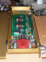
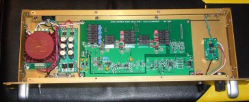
In your case, it's very important to verify correct assembly. I know you have checked - but most of us have a bit of psychological blindness when it comes to inspecting our own work. Sometimes it only takes a different pair of eyes to see a mistake. (Then you're on the hook to supply that person with a serving of his favorite malt beverage, in exchange for a promise that he will never tell your boss about the dumb mistake you made. Don't ask how I know about these things.) If you don't have a nearby friend in the hobby who can compare your unit to the assembly documentation, try posting clear, detailed photos as well as an assembly diagram or other documentation and perhaps a Forum member will notice an assembly error.
(Other members who have successfully assembled the project may be willing to post photos for comparison.)
Verifying supply voltages is an important first step in troubleshooting - good to know you have done that! Be sure to measure directly on the IC pins themselves. Occasionally, the voltage measured on a PWB pad will be different from the voltage on the component pin connected to the pad, due to a poor solder joint. (I have probably seen this more often with newly assembled SMT boards than thru-hole boards. For a variety of reasons the solder did not bridge between the pad and component, leaving a gap. Or the space filled up with excess flux rather than solder, leaving the component physically secured but electrically unconnected.)
If you have a 'scope, poke around on the PCB assembly to see if there are ANY signs of AC signals on the board. Of course, you'd like to find some very clean sinewaves but ANY kind of waveform, irregular transients, or even random noise could be clues to the basic fault.
For opamp circuits in general I like to look at the DC output voltages of each opamp. When I find one that's saturated a volt or two from a supply rail I carefully evaluate the signals on the INPUTS to that stage. In this case it may not be very helpful because the entire circuit is, by its nature, a closed-loop with net positive feedback. Even so you may find a stage where the opamp output voltage is not consistent with the input conditions, or where an input condition is incorrect due to an assembly error.
If you take DC voltage measurements it may be helpful to mark-up a copy of the schematic with the values. (As I mentioned, measure the DC voltage on both input pins as well as the output. Yes, the voltmeter probe will upset the behavior to some degree but you are looking for a significant problem(s), not finesse and subtlety.) People have different ways of perceiving patterns and visualizing data but for some it is helpful to see the "big picture" at a glance. Posting your annotated diagram may give somebody the insight to help find the problem.
I haven't looked up the schematic (it's from Glenn K, as I remember - may be appropriate to post a link to the latest version) but I think this is still a two-integrator state variable oscillator. At some point (after trying some other, simpler, ideas) it may be helpful to open the AC feedback loop (therefore turning it into an amplifier), inject a signal, and see if you get the gain necessary to sustain oscillation. I'd probably investigate that with a little simulation before trying it - not that I'm too worried about damaging components, but to give me a better feel for what to expect at various points in the circuit.
I recall that the level detector and AGC circuits in this project were extensively revised, and SIGNIFICANTLY more complex, from Bob Cordell's oscillator. If I had to make a seat-of-the-pants guess as to where your problem is most likely to reside, I'd look at the detector, error amp, and AGC circuits. The DC voltages on the gain control element (I think it's still a JFET, but may be an optocoupler) would be especially significant.
Bob Cordell's original "AUDIO" magazine articles for the THD analyzer are posted on his web site. Since this oscillator is a derivative of his work it may be helpful to skim those documents and see if they contain any troubleshooting hints.
Dale
Many incarnations ago I had a supervisor who was always telling the bench techs "Mech First!". Meaning, do a very thorough visual inspection of physical and mechanical characteristics before getting out any test equipment. Wiggle the wires, poke the components, prod the solder blobs, check fasteners for tightness, and look for signs of heat or physical damage. This often led you to the vicinity of a problem and saved diagnostic time.
In your case, it's very important to verify correct assembly. I know you have checked - but most of us have a bit of psychological blindness when it comes to inspecting our own work. Sometimes it only takes a different pair of eyes to see a mistake. (Then you're on the hook to supply that person with a serving of his favorite malt beverage, in exchange for a promise that he will never tell your boss about the dumb mistake you made. Don't ask how I know about these things.) If you don't have a nearby friend in the hobby who can compare your unit to the assembly documentation, try posting clear, detailed photos as well as an assembly diagram or other documentation and perhaps a Forum member will notice an assembly error.
(Other members who have successfully assembled the project may be willing to post photos for comparison.)
Verifying supply voltages is an important first step in troubleshooting - good to know you have done that! Be sure to measure directly on the IC pins themselves. Occasionally, the voltage measured on a PWB pad will be different from the voltage on the component pin connected to the pad, due to a poor solder joint. (I have probably seen this more often with newly assembled SMT boards than thru-hole boards. For a variety of reasons the solder did not bridge between the pad and component, leaving a gap. Or the space filled up with excess flux rather than solder, leaving the component physically secured but electrically unconnected.)
If you have a 'scope, poke around on the PCB assembly to see if there are ANY signs of AC signals on the board. Of course, you'd like to find some very clean sinewaves but ANY kind of waveform, irregular transients, or even random noise could be clues to the basic fault.
For opamp circuits in general I like to look at the DC output voltages of each opamp. When I find one that's saturated a volt or two from a supply rail I carefully evaluate the signals on the INPUTS to that stage. In this case it may not be very helpful because the entire circuit is, by its nature, a closed-loop with net positive feedback. Even so you may find a stage where the opamp output voltage is not consistent with the input conditions, or where an input condition is incorrect due to an assembly error.
If you take DC voltage measurements it may be helpful to mark-up a copy of the schematic with the values. (As I mentioned, measure the DC voltage on both input pins as well as the output. Yes, the voltmeter probe will upset the behavior to some degree but you are looking for a significant problem(s), not finesse and subtlety.) People have different ways of perceiving patterns and visualizing data but for some it is helpful to see the "big picture" at a glance. Posting your annotated diagram may give somebody the insight to help find the problem.
I haven't looked up the schematic (it's from Glenn K, as I remember - may be appropriate to post a link to the latest version) but I think this is still a two-integrator state variable oscillator. At some point (after trying some other, simpler, ideas) it may be helpful to open the AC feedback loop (therefore turning it into an amplifier), inject a signal, and see if you get the gain necessary to sustain oscillation. I'd probably investigate that with a little simulation before trying it - not that I'm too worried about damaging components, but to give me a better feel for what to expect at various points in the circuit.
I recall that the level detector and AGC circuits in this project were extensively revised, and SIGNIFICANTLY more complex, from Bob Cordell's oscillator. If I had to make a seat-of-the-pants guess as to where your problem is most likely to reside, I'd look at the detector, error amp, and AGC circuits. The DC voltages on the gain control element (I think it's still a JFET, but may be an optocoupler) would be especially significant.
Bob Cordell's original "AUDIO" magazine articles for the THD analyzer are posted on his web site. Since this oscillator is a derivative of his work it may be helpful to skim those documents and see if they contain any troubleshooting hints.
Dale
Hmm, no oscillation and everything in a fixed state if I get it right.
Have you checked the input/output potential at every op-amp? If (-) > (+) then output low and vice verse.
Hi Anders, I didn't get a chance to look at it yesterday. Maybe this morning I can fiddle with it.
Thank you so much for your long reply Dale! I really appreciate your time and attention on my little problem. Here's the schematic. He doesn't put voltages on their, so I'll have a poke around hopefully this morning. As I said, all the power supply voltages on each chip were correct. I didn't check the other things you mentioned yet. I can take closeup photos of the board and post them later.
Attachments
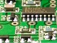
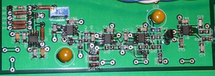
Here's a closeup of the voltage reference, error amplifier and nearby parts on the board. I got some voltages that look suspicious. First, there's 14VDC on pin 7 of U8 (the output), but very low voltages on pins 1 and 4 (inputs) of the same chip. There's also 13VDC on pin 2 of U9 (input). The other input is pin 3, which is connected to the above pin 7 @ 14VDC. So, I think there's something wrong with U8. I can't see any solder bridges, the chip doesn't get hot, and it's install correctly. Should I order another one and try to replace this one?
I noticed that the solder joint for pin 2 of U9 and U10 may not be perfect, but as I recall there was a solder bridge there so I used solder wick to clean it up. That usually doesn't cause a problem but who knows.
Thanks for everyone's help on this.
I noticed that the solder joint for pin 2 of U9 and U10 may not be perfect, but as I recall there was a solder bridge there so I used solder wick to clean it up. That usually doesn't cause a problem but who knows.
Thanks for everyone's help on this.
Attachments
Hi Dirk,
Great, one human error.")
Tune up? http://www.diyaudio.com/forums/group-buys/221670-sv-oscillator-pcb-group-buy-7.html#post3339959
Edit:
Check for signal prior to rectifier diodes at TP3, TP4. Switch frequencies and verify that both (all four) phases have signal.
Great, one human error.
Tune up? http://www.diyaudio.com/forums/group-buys/221670-sv-oscillator-pcb-group-buy-7.html#post3339959
Edit:
Check for signal prior to rectifier diodes at TP3, TP4. Switch frequencies and verify that both (all four) phases have signal.
Last edited:
Hi Dirk,
Great, one human error.
Tune up? http://www.diyaudio.com/forums/group-buys/221670-sv-oscillator-pcb-group-buy-7.html#post3339959
Edit:
Check for signal prior to rectifier diodes at TP3, TP4. Switch frequencies and verify that both (all four) phases have signal.
OK, Thanks.
So, I hook up TP2 to an FFT and adjust each of the 4 pots until it achieves a null on the second harmonic? I do this for every frequency?
Hi,
Each frequency group, see schematic for frequencies. Check FFT at TP2. Second will be obvious but other harmonics will follow.
Precaution, remove DC (cap) prior to your measurement device. Maybe obvious to you but better safe than sorry.
Oh, OK. I didn't look at the schematic. Each pot is for each frequency range. Got it. I didn't realize there was a lot of DC on TP2 and/or didn't think that the ADC I have should be AC coupled.
Thanks again!
Congratulations! Good work!I fixed it!
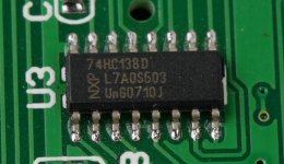
Please be careful with your verbal descriptions. You may need to re-calibrate your way of looking at things.There was a solder bridge across pins 2 and 3 of U8, neither of which are used by anything.
Those two pins ARE used for something! They are used to set the voltage gain of the instrumentation amplifier U8. It just so happens that leaving them open-circuit (i.e., no components connected to them) sets the voltage gain of U8 to 1 V/V. By connecting pin 2 to pin 3 (i.e., the short-circuit solder bridge) you set U8 to its maximum available voltage gain - something greater than 1000 V/V. (According to the formula in the Data Sheet the voltage gain would be infinite, but in reality the limitations of the physical part will limit the gain to something less than infinite.)
The part is specified to operate with voltage gains between 1 and 1000, so all bets are off regarding the part's behavior when the resistance between pin 2 and pin 3 is much less than 50 ohms or so. Operating with lower resistance between those pins, or even shorting them, is unlikely to cause damage to the IC.
Enjoy your new oscillator! It would be good to know if your unit has similar noise and distortion performance to Glenn's prototype.
Dale
- Status
- This old topic is closed. If you want to reopen this topic, contact a moderator using the "Report Post" button.
- Home
- Group Buys
- SV Oscillator PCB group buy