@ Andrea : thank you for the formule and the experience. So if we need to trigger, do we need a scope or is it possible with the ears like the Weber carburators of a Giuletta (no buzzzz in the speaker ? Sorry for the naive question!) ? Do you need to stay with the air trigger cap after finfing the good value or does exist a cap with the exact value (or very near) ?
@Crobbins : not surprised here : ok long legs but the good result of the Polypropylen ! The Wima or MKT I tried sounded very dry in my systems, 1 uF Bck ceramic too like John explained (resonances)... When I will make the DAC I will do a match between Polypro, Polysulfid, Polystyren and solid tantal ("+ leg" to Gnd) and the 2 refs John 's SM cap. It's DIY for me and i have already some big caps here
@Crobbins : not surprised here : ok long legs but the good result of the Polypropylen ! The Wima or MKT I tried sounded very dry in my systems, 1 uF Bck ceramic too like John explained (resonances)... When I will make the DAC I will do a match between Polypro, Polysulfid, Polystyren and solid tantal ("+ leg" to Gnd) and the 2 refs John 's SM cap. It's DIY for me and i have already some big caps here
There could be also some tolerances from batch to batch. E.g. I measured f = 12.000 kHz with C = 7500 pF, and from this I calculated R = 1.768 kohm and C = 510 pF for 176.4 kHz on my test setup. Another chip might have slightly different R, so it seems a variable capacitor for achieving the locking condition can't be avoided.The resistance of TDA1541 DEM RC oscillator should be around 1K85, so you can calculate the capacitor value for any frequency using the typical RC oscillator formula: c = 1 / (2 * Pi * 1850 * fDEM) (capacitance in Farad). Around 485 pF for 176kHz. BTW, I believe the resultant capacitor value has to be trimmed to lock (thanks James).
Yes, the internal R value has a tolerance, maybe it could vary within the same batch. That's the reason to use a variable cap in parallel with the fixed cap to fine tuning the lock condition. I have not yet tried, but seems the good practice was tuning the lock condition using a low level recording, ecdesigns, chris and james could explain how to do that.
Maybe, the best solution could be using a variable cap to determine the exact total cap value, measuring the total capacitance of both caps after tuning, then replace both with a fixed capacitor with the right value, that's means get the right capacitor from a big bag of them. I don't know how the final value is critical, a few pF or less, maybe someone could share his experience.
Anyone did try to sync the DEM clock at 88K2, starting with the WS signal followed by a frequency doubler? Strange idea, maybe someone could give a try.
I would be also interested in jitter measuring techniques in general.
Hi, oshifis, here is article.
Attachments
Please, Is there a method to lock with air cap trimer with ears (using speakers) or do we have to use a scope ? (no go for me)
You can play low volume music (-40db or lower). Once the dem oscillator locks, you will hear the music clearly. If it's not locked, you will hear digital noise.
Thank you Studio Stevus,
Because i will use the same source as you (SB receiver, if you have the opportunity to check one day the value of your 3 resistors in your I2S attenuation, it will be a pleasure to read you again...)
Super, I can beginn, i read, re-read and sometimes read again this post and I try to go with the last version with WS Soft DEM. So I have all but the I/V and the clock now. For the clock it's not a problem, I try to do the last version that ECdesigns (John) described or go to a kwak or Tentlab...
With OS and several cd players (TDA1541a or TDA 1540D) a too high value (>1uF) decoupling cap sound dry and harsch but this is OS and without change the running free sync Clock cap. 470nFdecoupling cap with the first 2 pins works fine for me with these two chips like the Philips LHH2000 but this is OS.
I don't understand the exact sound interaction between MSB decoupling cap & the sync clock cap in NOS mod... The higher the MSB, the Higher the clock cap = soft sound ? SSerg give me a doubt about the frequency and nobody report (but John) with the best match between frequency & MSB value. I surmise the proof of concept depends of the quality of the I/V stage and the rest of the hifi system...maybe and the quality of the cap surely!
I have to go to NOS now with this project and start with 1 uF Cornel Dublier SM cap first and will benchmark others caps when this project will make a sound (i hope!).
SO the I/V stage will be another story. Ihave a 100k input with my amplifier. But this chip is 30 years old and everybody is still talking about the ideal shematic after the tda1541... Gomez seems good even with modern tubes (Siemens D3A for 1st stage & ? for second). It seems a discrete can be good enough but this is the war here with NTD1, Cen, Zen, jocko,... I have to try but many times and money !
But it's a hobby, so thank you all for the advises and shematics, especially John here. I hope John comes back with new benchmarks with i/v stages.
cheers
Last edited:
Clarification on Attenuators with 3.3V source (incl. BCK)
Hi ECdesign and others,
I'd like to ask what should ideally be done with BCK when its fed from a 3.3V source.
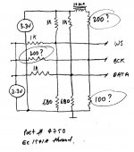
I can see that its amplitude will be about twice the level of WS and DATA (~1.7Vpp) when WS and DATA are using the 1k series and 1k + 680 voltage divider across the 3v3 supply.
From 3v3, (20 DCR inductor + 150R) +(100R) voltage divider would draw (3.3/270) = ~12mA and bias the input at ~1.2V when connected at the top of the 100R pull down resistor.
Is it then a simple matter of using 100R series resistor between the 3v3 BCK source and the top of that 100R pull down resistor (BCK/2) to reduce 3v3 BCK to ~1.65Vpp?
Is it close enough to be ok, or something else?.. (more series R, higher value pull down, higher value pull up, less current, same bias voltage, more attenuation ?)
Thanks,
Shane
Hi ECdesign and others,
crobbins5421 writes -"So for 3.3V application, BCK attenuation stays about the same with 5x 100R resistors, inductor, 220R pull-up, 68R pull down?..."
ecdesigns replies "In the latest projects I use a high speed / low jitter divide-by-4 circuit running on 1.8V (1.8Vpp output signal). I feed this 1.8Vpp BCK signal to the TDA154x using only a 180R series resistor.
I'd like to ask what should ideally be done with BCK when its fed from a 3.3V source.
I can see that its amplitude will be about twice the level of WS and DATA (~1.7Vpp) when WS and DATA are using the 1k series and 1k + 680 voltage divider across the 3v3 supply.
From 3v3, (20 DCR inductor + 150R) +(100R) voltage divider would draw (3.3/270) = ~12mA and bias the input at ~1.2V when connected at the top of the 100R pull down resistor.
Is it then a simple matter of using 100R series resistor between the 3v3 BCK source and the top of that 100R pull down resistor (BCK/2) to reduce 3v3 BCK to ~1.65Vpp?
Is it close enough to be ok, or something else?.. (more series R, higher value pull down, higher value pull up, less current, same bias voltage, more attenuation ?)
Thanks,
Shane
Last edited:
Since they are wideband digital signals, they should be handled in very particular way to conform digital signal transmission techniques such as impedance matching.
Your "divider" is basicly an attenuator which output impedance should be matched to the characteristic impedance of the trace (cable) you feed it thru, as long as it is being placed on the source of transmission line. It's source impedance is easily calculated of paraleling these 3 resistors.
Another way of dropping-off the level of signal is to terminate it in series at the source's end, make attenuator's input impedance the same as incoming transmission line, and source impedance the same as outgoing transmission line impedance... Much over my head i'd think, especially when you have to bias the output HI/LO voltages at particular level")
Your "divider" is basicly an attenuator which output impedance should be matched to the characteristic impedance of the trace (cable) you feed it thru, as long as it is being placed on the source of transmission line. It's source impedance is easily calculated of paraleling these 3 resistors.
Another way of dropping-off the level of signal is to terminate it in series at the source's end, make attenuator's input impedance the same as incoming transmission line, and source impedance the same as outgoing transmission line impedance... Much over my head i'd think, especially when you have to bias the output HI/LO voltages at particular level
Your "divider" is basicly an attenuator which output impedance should be matched to the characteristic impedance of the trace (cable) you feed it thru, as long as it is being placed on the source of transmission line. It's source impedance is easily calculated of paraleling these 3 resistors.
Thanks for this..
I'm a little confused because if the source impedance is the parallel value of the three resistors, consider the values of both WS and DATA 3k3//3k3//1k = 622ohms in the 5V attenuator cct, and 1k//1k//680 = 288 ohm in the 3v3 attenuator cct.
However, the values for WS and DATA have been given, and just BCK remains unknown (to me anyway). If I use the given values for the 5V cct 500//68//220 = ~47ohms.
If the attenuation is a function of the voltage divider created by the series resistor and the shunt resistor to ground, then signal level for WS and DATA in the 5V cct, after the divider, is 1.1V (this is Vpp?) and only 0.59V for BCK?.
If its desirable to have amplitude of the three lines between 1.2 and 1.4Vpp, and each biased between 1 and 1.4V, with a parallel resistor value of ~50 ohms for BCK, then the values I've arrived at are as in the attached image.
Does this all seem correct, or at least correct enough for the purpose, or have I got it all backwards?
Thanks,
Shane
Attachments
I was having the same issue, it was a bad divider chip. Once, I repaired it the erronious back ground noise disappeared to zero. On older recordings, I can pick out the actual background noise on the original analog recordings...
I am clocking DEM at 115khz, as I have a 48 bit word from a CD-Pro.
JohnK
I am clocking DEM at 115khz, as I have a 48 bit word from a CD-Pro.
JohnK
My DEM setup is not great (I still hear some digital noise in low volume passages), so would be looking forward to hear some ideas from others around this. I was quite happy with 176khz DEM frequency, but as mentioned, I have not set it up properly now....
Last edited:
Actually 132.3k but if I remember correctly.
I was having the same issue, it was a bad divider chip. Once, I repaired it the erronious back ground noise disappeared to zero. On older recordings, I can pick out the actual background noise on the original analog recordings...
I am clocking DEM at 115khz, as I have a 48 bit word from a CD-Pro.
JohnK
Hi Studiostevus,
As I see you are here, could you tell me please if you fed the clock in your SB receiver with the same value crystal you remove or do you use the more 12,8xxx (Xilinx Chip has tolerance ?)... I'm a little confuse to close my BOM list here !
thanks if you remember that...
As I see you are here, could you tell me please if you fed the clock in your SB receiver with the same value crystal you remove or do you use the more 12,8xxx (Xilinx Chip has tolerance ?)... I'm a little confuse to close my BOM list here !
thanks if you remember that...
Hi Studiostevus,
As I see you are here, could you tell me please if you fed the clock in your SB receiver with the same value crystal you remove or do you use the more 12,8xxx (Xilinx Chip has tolerance ?)... I'm a little confuse to close my BOM list here !
thanks if you remember that...
No problem,
I removed both crystals from the SB, and injected only the 11mhz clock signal from my dac board. Have a look at how John designed his clock earlier in this thread.
Ok, so 11 Mhz (value of the SB) and not the ~12,8 Mhz of John.
The last Clock design with a standalone crystal is not clear for me, the last shematic is the mk8 with 2 crystal use 12,8 Mhz. So I understand you use 11 Mhz for the SB. I believe i understand the two divide flip/flop chip for the TDA1541 BCK feeding. So i have to buy just one crystal of ~11 Mhz for the clock to inject in SB & TDA1541...
Internet is a good thing, we can be in the same pub even if we are far away...
Thank you Studiostevus
Last edited:
i guess, i have used earlier the mk7, which was 11mhz...Ok, so 11 Mhz (value of the SB) and not the ~12,8 Mhz of John.
There many clock designs on the web. One thing to take care of is to use buffered output which can drive 2 devices (in our case both the tda reclocker and the SB). John's mk7 is designed to drive 2 devices, namely the tda reclocker and his sd player, and is therefore very usefulThe last Clock design with a standalone crystal is not clear for me, the last shematic is the mk8 with 2 crystal use 12,8 Mhz. So I understand you use 11 Mhz for the SB. I believe i understand the two divide flip/flop chip for the TDA1541 BCK feeding. So i have to buy just one crystal of ~11 Mhz for the clock to inject in SB & TDA1541...
I didn't know that... for me bufered output & reciever was just for long wires... thank you for that.
I just have a look to my SB, the crystal are in fact ~22 Mhz, so I understand it's possible to "under"-feed a source with ~11, ~12 Mhz , etc. In my mind, it was a cause of jitter.
I assume it's possible too to go with 22Mhz with more divider for the TDA... but I have to copy a shematic if i want hear something... let's go for MK7 if the SB receiver works with it.
Actually use the old bck divider and level shift circuit to DEM.... Dividing down bck to 132.3k. I am also running 4x linear intorpolation with s1 chips.
Have 48bit word I2S word from a cdpro.
Have 48bit word I2S word from a cdpro.
What C value are you using between pin16 and 17? Somewhere around 700pF then, I assume?
- Home
- Source & Line
- Digital Line Level
- Building the ultimate NOS DAC using TDA1541A