Hi JOSI1,
I attached common mode regulator concept schematics for both, a positive and negative 5V supply.
John, can you share listening impressions of your voltage regs compared to other discrete alternatives?
I am designing a pcb now, based on many of your concepts, but with salas shunt regulators (most importantly to also add something of 'myself' and not to copy your whole design...). Not sure if i should pursue the salas regs or move towards your latest solution....
As far as I can see, John's Common Mode Regulator isolates both voltage supply and ground between the transformer/rectifier and the load.
Salas offers shunt regulator, which serves (probably successfully) a different purpose, which is supplying a very quiet voltage, but there is no isolation of the ground.
Possibly, a combination of both will be as good as it can be (especially for analog circuits).
However, when it comes to digital circuits, there is a huge benefit in isolating the power supply to each of the elements (clock, frequency divider, DAC chip, etc'). So, one shunt regulator to the entire unit may not be the best solution. Probably, a capacitance multiplier, or a separate regulator, to each of those building blocks is the best approach, since it does both functions in one stroke: supplying a very clean voltage and isolating different building blocks from one another.
Hi studiostevus,
The common mode voltage regulators result in a sound quality that closely approximates vinyl (without the scratches) and studio tape. With the discrete voltage regulators sound is already very good but one can still hear that the sound originates from a digital audio playback system.
The cascaded filtered buffered zener regulators in the form of a common mode regulator offer very fast local feedback and very low noise. They also provide essential high impedance between transformer / rectifier and connected load by placing a high impedance in the ground lead.
John, can you share listening impressions of your voltage regs compared to other discrete alternatives?
The common mode voltage regulators result in a sound quality that closely approximates vinyl (without the scratches) and studio tape. With the discrete voltage regulators sound is already very good but one can still hear that the sound originates from a digital audio playback system.
The cascaded filtered buffered zener regulators in the form of a common mode regulator offer very fast local feedback and very low noise. They also provide essential high impedance between transformer / rectifier and connected load by placing a high impedance in the ground lead.
Hi marconi118,
Yes, the new TDA1541A-MK8 will have 4 on-board common-mode regulators based on the filtered buffered zener regulator concept.
is the FET regulator of MK7 on post 3681 now obsolete?
Yes, the new TDA1541A-MK8 will have 4 on-board common-mode regulators based on the filtered buffered zener regulator concept.
Hi studiostevus,
The common mode voltage regulators result in a sound quality that closely approximates vinyl (without the scratches) and studio tape. With the discrete voltage regulators sound is already very good but one can still hear that the sound originates from a digital audio playback system.
I can add to this that we recently did a A/B listening comparison with my own full battery driven (4 x lead/acid) MK7 with discrete regulators against a same MK7 module with a experimental alpha version of the common mode voltage regulators on mains power. We did this test at John's place where the mains is pretty dirty. We could here NOT ANY DIFFERENCE between the batterie system and the mains PSU, how hard we tried. Incredible, a novum imo.
I can add to this that we recently did a A/B listening comparison with my own full battery driven (4 x lead/acid) MK7 with discrete regulators against a same MK7 module with a experimental alpha version of the common mode voltage regulators on mains power. We did this test at John's place where the mains is pretty dirty. We could here NOT ANY DIFFERENCE between the batterie system and the mains PSU, how hard we tried. Incredible, a novum imo.
Applauds to John.
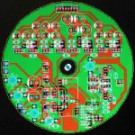
Here is a screen shot of the new TDA1541A-MK8 module PCB lay-out
It looks like it fits in a cd-player. Nice sentiment..

I can add to this that we recently did a A/B listening comparison with my own full battery driven (4 x lead/acid) MK7 with discrete regulators against a same MK7 module with a experimental alpha version of the common mode voltage regulators on mains power. We did this test at John's place where the mains is pretty dirty. We could here NOT ANY DIFFERENCE between the batterie system and the mains PSU, how hard we tried. Incredible, a novum imo.
you should try some truly low noise batteries, lead acid isnt exactly the leading edge of battery chemistries for audio. thats not a comment on the regulator design, which looks very interesting indeed and i'll definitely give it a try when more details are published. it could make for a nice alternative to batteries for the floating supplies for the CEN/SEN jfet IV stage by EUVL
it could make for a nice alternative to batteries for the floating supplies for the CEN/SEN jfet IV stage by EUVL
I was thinking the same. Let me know your results!
will do, it appears as though the darlingtons are end of supply at digikey, so adding some to my order now, i cant guaranty when i will get around to them though as i will be primarily focussing on batteries, but i WILL try them, dont really need any more detail either, cheap and simple to knock up and i think ive even got suitable zeners.
@ John, can buried zeners or other forms of reference be used for lower noise? i guess there is some reason you chose straight zeners though, no feedback perhaps?
@ John, can buried zeners or other forms of reference be used for lower noise? i guess there is some reason you chose straight zeners though, no feedback perhaps?
Last edited:
In the I2S attenuators, the diodes were replaced by a resistor. Resistor values were increased in order to reduce RF energy being dumped on the chip substrate. This allowed me to re-install the decoupling caps for WS and BCK reclockers.
BCK, Q: 100R, /Q: 470R, power supply series resistor: 470R, decoupling 1uF SMD film.
WS/DATA, Q: 470R, /Q: 2K2, power supply series resistor: 1K5, decoupling 1uF SMD film.
DEM injection: 2K2 / 12K
Masterclock: 100R with 1uF film bypass connected between GND and both chokes. This lifts the clock signal above GND and makes the clock rectifiers obsolete. The masterclock now runs on 2V power supply (4V minus 2V reference).
So, for bck, d5 and d6 are replaced by a 470r resistor, and 2k2 is added on the /q line... What are the resulting ttl levels?
Also, i remember i asked earlier why each flipflop was not decoupled separately. It seems in the current solution, they are? Or is it decoupling of the bck/ws/data lines themselves?
Hi brubeck,
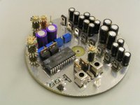
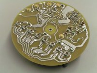
I attached some pictures of the TDA1541A-MK8 module that was completed today.
It looks like it fits in a cd-player. Nice sentiment..
I attached some pictures of the TDA1541A-MK8 module that was completed today.
Attachments
Hi John,
thank you for posting the schematics of the latest regulators and some pictures of the MK8 module.
In your designs you are using MELF resistors. Do these resistors have an electrical advantage compared to 0805/1210 or is it just for easier/better mounting and soldering?
thank you for posting the schematics of the latest regulators and some pictures of the MK8 module.
In your designs you are using MELF resistors. Do these resistors have an electrical advantage compared to 0805/1210 or is it just for easier/better mounting and soldering?
Hi studiostevus,
5 capacitors for each supply voltage, one smoothing cap and 4 more in the common mode capacitance multiplier. The power supply for the SD-player will have 5 isolated supply voltages, 4 for the DAC module and 1 for the SD-transport.
With the prototype setup I use 3 mains transformers, two transformers with 2 x 12V and one with 2 x 18V. Each common mode capacitance multiplier is connected to a separate transformer winding so all power supplies are "floating". The masterclock power supply is derived from a 18V winding using a couple of 100 Ohm resistors between transformer and rectifier in order to get required voltage on the common mode capacitance multiplier.
Transformer #1 is used for TDA1541A +5V and -5V supply. Transformer #2 is used for TDA1541A -15V and +5V masterclock supply. Transformer #3 is used for 3.3V SD-transport supply.
With these values low = 0.42V, high = 1.98V. I am currently experimenting with different values to further reduce RF energy. MK8 module now has 2K2 and 4K7 installed. This results in low = 0.7V, high = 1.5V.
The MK8 has 1uF SMD film power supply decoupling caps on all flip-flops. This is possible because of the modified I2S attenuator circuit.
So are there still a lot of caps in front of the regulators?
5 capacitors for each supply voltage, one smoothing cap and 4 more in the common mode capacitance multiplier. The power supply for the SD-player will have 5 isolated supply voltages, 4 for the DAC module and 1 for the SD-transport.
With the prototype setup I use 3 mains transformers, two transformers with 2 x 12V and one with 2 x 18V. Each common mode capacitance multiplier is connected to a separate transformer winding so all power supplies are "floating". The masterclock power supply is derived from a 18V winding using a couple of 100 Ohm resistors between transformer and rectifier in order to get required voltage on the common mode capacitance multiplier.
Transformer #1 is used for TDA1541A +5V and -5V supply. Transformer #2 is used for TDA1541A -15V and +5V masterclock supply. Transformer #3 is used for 3.3V SD-transport supply.
So, for bck, d5 and d6 are replaced by a 470r resistor, and 2k2 is added on the /q line... What are the resulting ttl levels?
With these values low = 0.42V, high = 1.98V. I am currently experimenting with different values to further reduce RF energy. MK8 module now has 2K2 and 4K7 installed. This results in low = 0.7V, high = 1.5V.
Also, i remember i asked earlier why each flipflop was not decoupled separately. It seems in the current solution, they are? Or is it decoupling of the bck/ws/data lines them
The MK8 has 1uF SMD film power supply decoupling caps on all flip-flops. This is possible because of the modified I2S attenuator circuit.
- Home
- Source & Line
- Digital Line Level
- Building the ultimate NOS DAC using TDA1541A