Hi zjaakco,
Jitter is a distortion in the time domain, here is a link that contains a simplified visual representation of jitter:
Low-Jitter Oscillator : LessLoss high end audio power cables, audiophile power cables, audiophile cables
Jitter is a distortion in the time domain, here is a link that contains a simplified visual representation of jitter:
Low-Jitter Oscillator : LessLoss high end audio power cables, audiophile power cables, audiophile cables
Hi, ECD,
I have read the link a few times, emh, I still don't understand jitter.
I learned jitter is a distortion in time. And it seems very difficult
to explane jitter.
I found this, Informatie over de zin en onzin in high-end hifi techniek, with a English link.
Ecd thanks a lot.
Best regards
Zjaakco
I have read the link a few times, emh, I still don't understand jitter.
I learned jitter is a distortion in time. And it seems very difficult
to explane jitter.
I found this, Informatie over de zin en onzin in high-end hifi techniek, with a English link.
Ecd thanks a lot.
Best regards
Zjaakco
Hi zjaako,
Here is another link:
Digital Interfaces - An Introduction - Part 1.1 [English]
There are 5 parts.
I know a lot of nonsense is told about High-End audio equipment. But most of the statements made in the section "sense and nonsense about High-End audio equipment" are simply wrong.
Hi, ECD,
I have read the link a few times, emh, I still don't understand jitter.
I learned jitter is a distortion in time. And it seems very difficult
to explane jitter.
Here is another link:
Digital Interfaces - An Introduction - Part 1.1 [English]
There are 5 parts.
I found this, Informatie over de zin en onzin in high-end hifi techniek, with a English link.
I know a lot of nonsense is told about High-End audio equipment. But most of the statements made in the section "sense and nonsense about High-End audio equipment" are simply wrong.
-ecdesigns-; said:But most of the statements made in the section "sense and nonsense about High-End audio equipment" are simply wrong.
mr. Breem unmasked?

Hi ECD,
Thanks for your reaction. The link to breem.nl, I mentioned it,
because there to is an explanation of jitter. I have no interest in his
audio statement about right or false. Just on this forum I learn a
lot about audio, but still I be critical. Mine knowlegd about digital is very less. This thread was running a few years before I picked it up. Better late than never!!
Best regards
Zjaakco
Hi zjaakco,
Jitter is a distortion in the time domain, here is a link that contains a simplified visual representation of jitter:
Low-Jitter Oscillator : LessLoss high end audio power cables, audiophile power cables, audiophile cables

Hi, ECD,
I have read the link a few times, emh, I still don't understand jitter.
I learned jitter is a distortion in time. And it seems very difficult
to explane jitter.
I found this, Informatie over de zin en onzin in high-end hifi techniek, with a English link.
Ecd thanks a lot.
Best regards
Zjaakco
It might help to think about jitter in the following way. While jitter is a time error prior to D/A conversion, it manifests as an amplitude error after D/A conversion. Jitter produces the right signal amplitude but at the wrong moment in time after D/A conversion, which is equivalent to jitter producing the wrong amplitude at the right moment in time after D/A. Hopefully, this helps reveal that jitter produces an amplitude error/distortion as it reaches our ears.
Therefore, jitter can be suppressed via either time-base stabilization, or by pre-distorting (correcting) the sample amplitude error which would otherwise manifest after D/A conversion. That latter solution, pre-distorting the signal amplitude error is how ASRC technology suppresses jitter.
Last edited:
Hi ECD
This, Digital Interfaces - An Introduction - Part 1.1 [English] , is indeed a good explanation of jitter .
Oshifis, Ken Newton. Drubeck. tanks for your reaction.
Regards
Zjaakco
This, Digital Interfaces - An Introduction - Part 1.1 [English] , is indeed a good explanation of jitter .
Oshifis, Ken Newton. Drubeck. tanks for your reaction.
Regards
Zjaakco
I attached a photograph of TDA1541A hardwired decoupling.
Red indicates +5V decoupling to AGND (pin 5)
Blue indicates -5V decoupling to AGND (pin5)
Purple indicates -15V decoupling to AGND (pin 5)
Yellow indicates left channel active divider decoupling to AGND (pin 5)
Orange indicates right channel active divider decoupling to AGND (pin 5)
Pins 4 and 5 are connected for convenience (pin 4 is nc on the TDA1541A).
Light blue indicates GND plane connection between DGND (pin 14) and AGND (pin5).
I performed some experiments connecting only the -5V (digital supply) decoupling to DGND, but listening tests showed a preference for decoupling to AGND.
With this wiring method, a local star ground is created at pin 4 / 5. This minimizes crosstalk between all connected GND wires as shared GND return paths are avoided.
Hi John,
The quote is from your post #3820 from 7th September.
What capacitors do you use?
Also, are there any news about MK7 power supply?
Hi Joshua_G
1uF/16V 1210 size SMD film caps from Cornell Dubilier.
I completed design and testing of the common-mode power supply. There is a separate common-mode power supply for each voltage. The common-mode power supplies now consist of a common-mode ripple rejector circuit followed by a common-mode filtered buffered zener diode regulator based on one or more zener diodes and a single Darlington transistor. The post regulator that is part of the common-mode regulator is now placed as close to DAC chip and masterclock as possible.
The task of the common mode power supply is placing a high impedance between mains transformer and connected circuit. This requires a high impedance in both, plus / minus and GND. The power supply first attenuates rectifier ripple voltage and interference by two cascaded ripple rejector circuits, one in plus / minus line, the other in GND. These are followed by two cascaded filtered buffered zener diode regulators. The pre regulator is placed in the GND line, the post regulator is placed on the DAC module in plus / minus lines.
The common mode power supplies are required to tackle the ever increasing interference on the mains and the effect of ground loops.
I am currently testing the TDA1541A-MK8 prototype setup that is powered by the common-mode power supplies. Perceived sound quality is so natural, relaxing and refined that it takes some time to get used to it.
In the MK8, all diodes were removed from I2S attenuators, DEM injector and masterclock (rectifiers). Listening tests showed that the amount of semiconductors are best reduced to absolute minimum.
In the I2S attenuators, the diodes were replaced by a resistor. Resistor values were increased in order to reduce RF energy being dumped on the chip substrate. This allowed me to re-install the decoupling caps for WS and BCK reclockers.
BCK, Q: 100R, /Q: 470R, power supply series resistor: 470R, decoupling 1uF SMD film.
WS/DATA, Q: 470R, /Q: 2K2, power supply series resistor: 1K5, decoupling 1uF SMD film.
DEM injection: 2K2 / 12K
Masterclock: 100R with 1uF film bypass connected between GND and both chokes. This lifts the clock signal above GND and makes the clock rectifiers obsolete. The masterclock now runs on 2V power supply (4V minus 2V reference).
BCK is derived directly from the masterclock using a divide_by_4 circuit.
The post regulators for DAC and masterclock power supply will be placed on the MK8 module.
Decoupling caps for the TDA1541A will now be soldered directly on the chip instead of the PCB. This improves required RF decoupling.
The MK8 PCB was changed to a disc shape for a number of reasons like segmenting / screening sub circuits, integrated mechanical damping mechanism, and an attempt to integrate a Mobius GND surface that should offer very low inductance. The aim of the Mobius GND surface is further reduction of RF ground noise.
What capacitors do you use?
1uF/16V 1210 size SMD film caps from Cornell Dubilier.
Also, are there any news about MK7 power supply?
I completed design and testing of the common-mode power supply. There is a separate common-mode power supply for each voltage. The common-mode power supplies now consist of a common-mode ripple rejector circuit followed by a common-mode filtered buffered zener diode regulator based on one or more zener diodes and a single Darlington transistor. The post regulator that is part of the common-mode regulator is now placed as close to DAC chip and masterclock as possible.
The task of the common mode power supply is placing a high impedance between mains transformer and connected circuit. This requires a high impedance in both, plus / minus and GND. The power supply first attenuates rectifier ripple voltage and interference by two cascaded ripple rejector circuits, one in plus / minus line, the other in GND. These are followed by two cascaded filtered buffered zener diode regulators. The pre regulator is placed in the GND line, the post regulator is placed on the DAC module in plus / minus lines.
The common mode power supplies are required to tackle the ever increasing interference on the mains and the effect of ground loops.
I am currently testing the TDA1541A-MK8 prototype setup that is powered by the common-mode power supplies. Perceived sound quality is so natural, relaxing and refined that it takes some time to get used to it.
In the MK8, all diodes were removed from I2S attenuators, DEM injector and masterclock (rectifiers). Listening tests showed that the amount of semiconductors are best reduced to absolute minimum.
In the I2S attenuators, the diodes were replaced by a resistor. Resistor values were increased in order to reduce RF energy being dumped on the chip substrate. This allowed me to re-install the decoupling caps for WS and BCK reclockers.
BCK, Q: 100R, /Q: 470R, power supply series resistor: 470R, decoupling 1uF SMD film.
WS/DATA, Q: 470R, /Q: 2K2, power supply series resistor: 1K5, decoupling 1uF SMD film.
DEM injection: 2K2 / 12K
Masterclock: 100R with 1uF film bypass connected between GND and both chokes. This lifts the clock signal above GND and makes the clock rectifiers obsolete. The masterclock now runs on 2V power supply (4V minus 2V reference).
BCK is derived directly from the masterclock using a divide_by_4 circuit.
The post regulators for DAC and masterclock power supply will be placed on the MK8 module.
Decoupling caps for the TDA1541A will now be soldered directly on the chip instead of the PCB. This improves required RF decoupling.
The MK8 PCB was changed to a disc shape for a number of reasons like segmenting / screening sub circuits, integrated mechanical damping mechanism, and an attempt to integrate a Mobius GND surface that should offer very low inductance. The aim of the Mobius GND surface is further reduction of RF ground noise.
Hi John,
For the past few weeks I read this thread from the beginning. I'm in a great appreciation of your continues endeavors over 5 and a half years to achieve a better sounding DAC. I believe that every new generation sounds better than the previous one.
It looks to me that you are on the right tracks, starting with the best sounding DAC chip and than implementing quietest possible voltages supply and quietest and most stable possible signals.
As for your discrete regulators, possibly plain capacitance multipliers will be quieter. They can get even quieter when for low power consumption clients the pass elements can be JFETs like 2SK170 and 2SJ74, possibly few JFETs in parallel. Just an idea.
Also, sometimes multilayer PCBs with ground planes on the inner layers help minimizing high frequency interferences.
Will your MK8 DAC have an option for balanced output (to be used in all balanced sound systems)?
Will your SD Card Reader / DAC combo have an option for an additional external SPDIF and/or I2S source? I'm well aware of jitter and noise problems from external sources, yet, your DAC will most probably be the best sounding one for external sources, with all their inherent drawbacks and limitations.
MK8...story goes on
Hi ecdesigns,
soldering the decoupling caps directly to the chip-pins is a logical decision in your design process. If I remember right, "nazar" - here in the forum - did the same, using 4µ7-X7R, see his "DAC Overture V2.3".
A mechanical idea could be to use a pure copper shield(size ~1mm) on top of the TDA chip for an individual groundplane in chip-size.
All decoupling caps = pin : 28-27,26,24,23,22,21,20,19,18,15 and 14,13,12,11,10,9,8,7,5-4 are soldered together on this groundplane, connected from pin 4-5 to common ground.
So all individual TDA currents can flow and resistance and inductive reactance are minimised.
Just an idea, may be helpful.
Regards Harry
Hi,
I did precisely this in my 1998 TDA1541 DAC project known as "Adagio".
I wrapped the TDA into heavy, self adhesive copper foil and soldered all decoupling caps directly to the pin's and that.
The whole assembly was the soldered dead bug style to a piece of PCB material to which the bigger decoupling caps and TL431 Shunt regulators where attached.
Certainly resulted in very low measured noise on the supply lines...
Ciao T
A mechanical idea could be to use a pure copper shield(size ~1mm) on top of the TDA chip for an individual groundplane in chip-size.
All decoupling caps = pin : 28-27,26,24,23,22,21,20,19,18,15 and 14,13,12,11,10,9,8,7,5-4 are soldered together on this groundplane, connected from pin 4-5 to common ground.
I did precisely this in my 1998 TDA1541 DAC project known as "Adagio".
I wrapped the TDA into heavy, self adhesive copper foil and soldered all decoupling caps directly to the pin's and that.
The whole assembly was the soldered dead bug style to a piece of PCB material to which the bigger decoupling caps and TL431 Shunt regulators where attached.
Certainly resulted in very low measured noise on the supply lines...
Ciao T
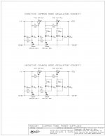
Common mode power supply concept schematics
Hi JOSI1,
I attached common mode regulator concept schematics for both, a positive and negative 5V supply.
Hi JOSI1,
can You show in more detail how the common-mode filtered buffered zener diode regulator looks like when placed in both supply lines. Is the circuit for the pre regulator (GND line) and the post regulator (Plus/minus line) identical?
I attached common mode regulator concept schematics for both, a positive and negative 5V supply.
Attachments
Hi Joshua_G
The pass elements for both, capacitance multiplier and filtered buffered zener regulators need to have high gain, low voltage drop and high (surge) current capability. This makes 2SK170 and 2SJ74 less suitable.
When a curtrent flows from point A to point B in a PCB trace located above a ground plane, one cannot guarantee that the return current flows back exactly the same way.
Multiple return currents will now flow through the ground plane, choosing the momentary path of lowest impedance. This in turn creates increased EM levels and unwanted coupling between signals sharing the same GND return plane.
Better method is providing a well defined GND return path for each signal, ensuring optimal canceling of EM fields and minimizing coupling between multiple GND return signals.
No, The MK8 will have single-ended DC-coupled output like the MK7 because there is no need for balanced outputs when using short interlinks and common mode supplies that minimize ground loop issues.
This would increase SD-player complexity and would also significantly degrade SD-player performance when both SPDIF and USB interfaces weren't used / disabled.
Since I strive for most basic straight-forward approach and highest possible performance, I simply refuse to add these interfaces to the SD-player.
As for your discrete regulators, possibly plain capacitance multipliers will be quieter. They can get even quieter when for low power consumption clients the pass elements can be JFETs like 2SK170 and 2SJ74, possibly few JFETs in parallel. Just an idea.
The pass elements for both, capacitance multiplier and filtered buffered zener regulators need to have high gain, low voltage drop and high (surge) current capability. This makes 2SK170 and 2SJ74 less suitable.
Also, sometimes multilayer PCBs with ground planes on the inner layers help minimizing high frequency interferences.
When a curtrent flows from point A to point B in a PCB trace located above a ground plane, one cannot guarantee that the return current flows back exactly the same way.
Multiple return currents will now flow through the ground plane, choosing the momentary path of lowest impedance. This in turn creates increased EM levels and unwanted coupling between signals sharing the same GND return plane.
Better method is providing a well defined GND return path for each signal, ensuring optimal canceling of EM fields and minimizing coupling between multiple GND return signals.
Will your MK8 DAC have an option for balanced output (to be used in all balanced sound systems)?
No, The MK8 will have single-ended DC-coupled output like the MK7 because there is no need for balanced outputs when using short interlinks and common mode supplies that minimize ground loop issues.
Will your SD Card Reader / DAC combo have an option for an additional external SPDIF and/or I2S source? I'm well aware of jitter and noise problems from external sources, yet, your DAC will most probably be the best sounding one for external sources, with all their inherent drawbacks and limitations.
This would increase SD-player complexity and would also significantly degrade SD-player performance when both SPDIF and USB interfaces weren't used / disabled.
Since I strive for most basic straight-forward approach and highest possible performance, I simply refuse to add these interfaces to the SD-player.
- Home
- Source & Line
- Digital Line Level
- Building the ultimate NOS DAC using TDA1541A