oscillograms
Hi John,
I suggest you to use a digital scope of a good quality. I've been using analog ones for a lot of years, but when I've switched to digital, for some sensitive measurements, like oscillators and digital signals, it work vasty better, respect to amplitud sensitivity and the precise shape of the wave. You can even measure quickly the frequency and amplitude. Give it a try. Probably, you will see that the signals are worst that the ones you see with your actual scope.
Kind regards.
Hi Studiostevus,
You may want to consider finding someone with a higher bandwidth scope to visit and take some measurements. With your 50MHz maximum scope bandwidth, the fast edges may not be as rounded as pictured on your screen shot. Make sure you are not using a low bandwidth probe as well...
If that is a 10ns rise time edge in John's picture, a 100MHz bandwidth scope would be nice to see what it is really looks like. 50MHz just barely makes it. I reality, the edge in John's circuit is probably on the order of only a few nS and the wave shape may be somewhat bandwidth limited in his photos as well. Just as an example - A 1nS rise time requires a 500MHz scope bandwidth (and probe bandwidth) minimum in practice, 1GHz would be optimal.
This note gives a quick overview of bandwidth requirements and has some pictures of what scope bandwidth limits can do to a digital waveform. The same signal is captured with scopes of increasing bandwidth: http://cp.literature.agilent.com/litweb/pdf/5989-5733EN.pdf
It is also important to use good scope grounding techniques - Don't use the ground lead. Put a tip ground on the probe and find a ground close to the measurement point. This keeps the measurement path coaxial as much as is possible to minimize the effects of stray noise and ground currents polluting the measurement.
Hope it helps,
Dave
Just a suggestion here - The pictures look like they may be bandwidth limited measurements.Thanks John. So it seems the mosfet buffer is not working correctly.
I measured and checked my pcb again. Everything seems to be wired correctly.
A faulty SK216 could be the culprit.. although 2 faulty ones seems highly unlikely...
You may want to consider finding someone with a higher bandwidth scope to visit and take some measurements. With your 50MHz maximum scope bandwidth, the fast edges may not be as rounded as pictured on your screen shot. Make sure you are not using a low bandwidth probe as well...
If that is a 10ns rise time edge in John's picture, a 100MHz bandwidth scope would be nice to see what it is really looks like. 50MHz just barely makes it. I reality, the edge in John's circuit is probably on the order of only a few nS and the wave shape may be somewhat bandwidth limited in his photos as well. Just as an example - A 1nS rise time requires a 500MHz scope bandwidth (and probe bandwidth) minimum in practice, 1GHz would be optimal.
This note gives a quick overview of bandwidth requirements and has some pictures of what scope bandwidth limits can do to a digital waveform. The same signal is captured with scopes of increasing bandwidth: http://cp.literature.agilent.com/litweb/pdf/5989-5733EN.pdf
It is also important to use good scope grounding techniques - Don't use the ground lead. Put a tip ground on the probe and find a ground close to the measurement point. This keeps the measurement path coaxial as much as is possible to minimize the effects of stray noise and ground currents polluting the measurement.
Hope it helps,
Dave
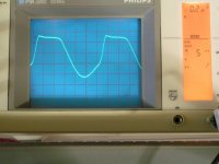
Hi fitzfish,
These were made using a Hameg HM604-3 (2 x 60 MHz) scope, HF probe, using probe ground lead. This scope is now defective so no more 60 MHz measurements")
My brand new Hameg 1500-2 developed faults after using it few times and is returned for repair.
I repeated the measurement using a Philips / Fluke PM3065 (2 x 100 MHz) using short (1cm) ground lead soldered between probe tip GND and circuit GND. Time base on maximum setting (x 10), manually adjusted for best fit. I attached the oscillogram (signal before clock rectifiers). With original probe ground lead I get ringing on the signal (as expected), similar as with the HM604-3 measurement.
Just a suggestion here - The pictures look like they may be bandwidth limited measurements.
These were made using a Hameg HM604-3 (2 x 60 MHz) scope, HF probe, using probe ground lead. This scope is now defective so no more 60 MHz measurements
My brand new Hameg 1500-2 developed faults after using it few times and is returned for repair.
I repeated the measurement using a Philips / Fluke PM3065 (2 x 100 MHz) using short (1cm) ground lead soldered between probe tip GND and circuit GND. Time base on maximum setting (x 10), manually adjusted for best fit. I attached the oscillogram (signal before clock rectifiers). With original probe ground lead I get ringing on the signal (as expected), similar as with the HM604-3 measurement.
Attachments
John,
With respect, if I make this kind of measurements I use a 100:1 probe (that is average 1pF input capacitance) AND a differential clip on (the springy thing that replaces the ground lead completely). That is quite independent of scope and bandwidth. Even with these measures I have low confidence that what I see is actually what happens...
Ciao T
I repeated the measurement using a Philips / Fluke PM3065 (2 x 100 MHz) using short (1cm) ground lead soldered between probe tip GND and circuit GND.
With respect, if I make this kind of measurements I use a 100:1 probe (that is average 1pF input capacitance) AND a differential clip on (the springy thing that replaces the ground lead completely). That is quite independent of scope and bandwidth. Even with these measures I have low confidence that what I see is actually what happens...
Ciao T
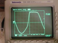
Hi John,
Thanks for the additional captures. The look more realistic on the faster scopes. Duty cycle is now symmetrical and the FET vgs flat top does not have the overshoot.
Seeing the pictures makes the circuit operation easy to understand. Very cool application of the fast FET! It would be interesting to see what the real risetime after the rectifiers is if you were ever able to measure it with a high bandwidth setup.
Dave
Hi fitzfish,
The FET is a lateral audio MOSFET (2SK216), 200V, 500mA, 1.75W, Ysf 40mS, input capacitance 90pF, reverse transfer capacitance 2.2pF. I chose this MOSFET because of noise spectrum (lower noise in the audio band). Most large bandwidth FETs and transistors have low noise outside the audio band but increased noise within the audio band. I also noticed that devices with higher power (chip bonded to a heatsink) performed better, could be caused by thermal memory effects.
The rise time after the rectifiers is similar to the rise time of the signal on the source of the MOSFET. This was achieved by using fast RF Schottky diodes:
AVAGO TECHNOLOGIES|HSMS-2800-TR1G|DIODE, RF, SCHOTTKY, SOT-23 | Farnell Nederland
Clock signal wave shape is one thing, achieving lowest possible jitter is much more important.
In order to minimize jitter with this balanced masterclock it is important to connect only one clock load with lowest possible load capacitance to each output, keeping wiring as short as possible.
The masterclock power supply is also highly critical. It needs to be an extremely "quiet" power supply that remains quiet during sudden load fluctuations.
It is also important to use a separate power supply for the masterclock, I recently changed this in the MK7.
Seeing the pictures makes the circuit operation easy to understand. Very cool application of the fast FET! It would be interesting to see what the real risetime after the rectifiers is if you were ever able to measure it with a high bandwidth setup.
The FET is a lateral audio MOSFET (2SK216), 200V, 500mA, 1.75W, Ysf 40mS, input capacitance 90pF, reverse transfer capacitance 2.2pF. I chose this MOSFET because of noise spectrum (lower noise in the audio band). Most large bandwidth FETs and transistors have low noise outside the audio band but increased noise within the audio band. I also noticed that devices with higher power (chip bonded to a heatsink) performed better, could be caused by thermal memory effects.
The rise time after the rectifiers is similar to the rise time of the signal on the source of the MOSFET. This was achieved by using fast RF Schottky diodes:
AVAGO TECHNOLOGIES|HSMS-2800-TR1G|DIODE, RF, SCHOTTKY, SOT-23 | Farnell Nederland
Clock signal wave shape is one thing, achieving lowest possible jitter is much more important.
In order to minimize jitter with this balanced masterclock it is important to connect only one clock load with lowest possible load capacitance to each output, keeping wiring as short as possible.
The masterclock power supply is also highly critical. It needs to be an extremely "quiet" power supply that remains quiet during sudden load fluctuations.
It is also important to use a separate power supply for the masterclock, I recently changed this in the MK7.
It is also important to use a separate power supply for the masterclock, I recently changed this in the MK7.
John, did you separate the masterclock power supply from the reclocker (flipflops) power supply?
I am running those on the same regulated supply (of course separated from the TDA supplies, however they are on the same transformer). In my final version will see if I can use a completely isolated supply for clock+flipflops, up to the transformer.
An externally hosted image should be here but it was not working when we last tested it.
Fitzfish.... looking again at my own scope measurements (50 Mhz) and comparing with ECDesigns (100 Mhz), there are so many differences that I am still suspecting that there is something in the circuit, not only in the measurements...
Hi John,
I look forward to building one of these oscillators at some point and measuring it.
Thanks again,
Dave
All makes good sense. Can you share how you characterize FETs for noise in this band?I chose this MOSFET because of noise spectrum (lower noise in the audio band). Most large bandwidth FETs and transistors have low noise outside the audio band but increased noise within the audio band. I also noticed that devices with higher power (chip bonded to a heatsink) performed better, could be caused by thermal memory effects.
Absolutely agree. I brought up the waveform shape only as an indicator of how well the measurement setup performed.Clock signal wave shape is one thing, achieving lowest possible jitter is much more important.
I look forward to building one of these oscillators at some point and measuring it.
Thanks again,
Dave
Hi Studiostevus,
What is the bandwidth and capacitance of the probe you are using?
Is the scope set to 1M ohm input?
Do you have a ground plane under the entire circuit and are you probing with the ground tip adapter, not the ground wire with the clip on the end?
Are the inductors correct?
Is the power supply current limiting?
If none of the above is helpful, would you care to post pictures of the circuit and probing technique to see if anyone can spot an issue?
Dave
It is possible it's not working correctly. I would still venture to guess that it is working better than it appears in the picture and there is a measurement issue. It still looks like the circuit is charging a relatively substantial reactance (tens of picofarads would be my guess)...Fitzfish.... looking again at my own scope measurements (50 Mhz) and comparing with ECDesigns (100 Mhz), there are so many differences that I am still suspecting that there is something in the circuit, not only in the measurements...
What is the bandwidth and capacitance of the probe you are using?
Is the scope set to 1M ohm input?
Do you have a ground plane under the entire circuit and are you probing with the ground tip adapter, not the ground wire with the clip on the end?
Are the inductors correct?
Is the power supply current limiting?
If none of the above is helpful, would you care to post pictures of the circuit and probing technique to see if anyone can spot an issue?
Dave
Hi John,
Thanks,
Dave
Will you share the vendor/part number for the bobbin as well as winding details for the multi-segment inductor?They are custom made screened 4-segment 100uH air chokes (attached photograph). The reason for using multiple segments is to minimize stray capacitance.
Thanks,
Dave
Did some more measurements with local GND and different scope settings. Now the trace somewhat resembles ECD's. The rest is probably indeed due to limited scope bandwidth.Hi Studiostevus,
It is possible it's not working correctly. I would still venture to guess that it is working better than it appears in the picture and there is a measurement issue. It still looks like the circuit is charging a relatively substantial reactance (tens of picofarads would be my guess)...
What is the bandwidth and capacitance of the probe you are using?
Is the scope set to 1M ohm input?
Do you have a ground plane under the entire circuit and are you probing with the ground tip adapter, not the ground wire with the clip on the end?
Are the inductors correct?
Is the power supply current limiting?
If none of the above is helpful, would you care to post pictures of the circuit and probing technique to see if anyone can spot an issue?
Dave
thanks for your help

Hi Fitzfish,
I glued two Epcos/Siemens P14/013/9 coilformers (2 sections) together using bison transparent glue. I centered the coil formers using the round wooden handle of a small paint brush. This creates a 4 section coil former with 6mm diameter and 4 sections of 2mm high.
Here is a link for this coil former:
Menting Mikroelektrik - P 14 Spulenkörper, 2 Kammern, volle Höhe
The winding consists of 4 x 50 windings of 0.1 ... 0,2mm enameled copper wire.
The value measured with my Hameg LCR meter equals approx. 140uH.
This air choke is then placed in a shield that is often used for shielding IF transformers in radio's. They look like this:
If Transformer Coil Toko
I removed the IF transformer and only used the shield.
Will you share the vendor/part number for the bobbin as well as winding details for the multi-segment inductor?
I glued two Epcos/Siemens P14/013/9 coilformers (2 sections) together using bison transparent glue. I centered the coil formers using the round wooden handle of a small paint brush. This creates a 4 section coil former with 6mm diameter and 4 sections of 2mm high.
Here is a link for this coil former:
Menting Mikroelektrik - P 14 Spulenkörper, 2 Kammern, volle Höhe
The winding consists of 4 x 50 windings of 0.1 ... 0,2mm enameled copper wire.
The value measured with my Hameg LCR meter equals approx. 140uH.
This air choke is then placed in a shield that is often used for shielding IF transformers in radio's. They look like this:
If Transformer Coil Toko
I removed the IF transformer and only used the shield.
Hi studiostevus,
No, I use one common-mode 5V supply for masterclock, BCK divider and WS / DATA reclockers.
The voltage levels after passive RC filtering / voltage attenuation are:
Masterclock: 4V (40 Ohm, 2uF)
BCK divider: 2.4V (680 Ohm, 2uF)
WS synchronous reclocker: 2.4V (1K5)
DATA synchronous reclocker: 2.4V (1K5)
These voltages may differ slightly depending on actual chip and masterclock power consumption.
John, did you separate the masterclock power supply from the reclocker (flipflops) power supply?
No, I use one common-mode 5V supply for masterclock, BCK divider and WS / DATA reclockers.
The voltage levels after passive RC filtering / voltage attenuation are:
Masterclock: 4V (40 Ohm, 2uF)
BCK divider: 2.4V (680 Ohm, 2uF)
WS synchronous reclocker: 2.4V (1K5)
DATA synchronous reclocker: 2.4V (1K5)
These voltages may differ slightly depending on actual chip and masterclock power consumption.
Hi dutchaudio,
More detailed information about this chip can be found in IEEE Journal of Solid State Circuits, vol. sc-21, June 1986.
http://www.dutchaudioclassics.nl/Philips-TDA1541_A-Monolithic-Dual-16-Bit-D-A-Converter/
Hi Fitzfish,
I glued two Epcos/Siemens P14/013/9 coilformers (2 sections) together using bison transparent glue. I centered the coil formers using the round wooden handle of a small paint brush. This creates a 4 section coil former with 6mm diameter and 4 sections of 2mm high.
Here is a link for this coil former:
Menting Mikroelektrik - P 14 Spulenkörper, 2 Kammern, volle Höhe
The winding consists of 4 x 50 windings of 0.1 ... 0,2mm enameled copper wire.
The value measured with my Hameg LCR meter equals approx. 140uH.
This air choke is then placed in a shield that is often used for shielding IF transformers in radio's. They look like this:
If Transformer Coil Toko
I removed the IF transformer and only used the shield.
Thanks John.
I'll see if I can find the forms or something similar here.
Dave
jitter?
Hi ECD
I have read close on your tread. Still I am some confused about
jitter. The next is only for clarity for me.
Jitter is distortion in time. for example, if a square wave start running vertical, the time start running horizontal. This mean the up going signal get some slantingly. The signal come to his maximum, the signal runs parallel with the time, and if it go down the signal go again some slantingly. So, 2 times a small shift in time. Is this indeed jitter?
Regards
Zjaakco
- Home
- Source & Line
- Digital Line Level
- Building the ultimate NOS DAC using TDA1541A