CeeVee,
I agree with your post above. Delete the holes under the part, they do not contribute all that much. The holes under the “wings” or finned area are the most important and should be made big enough that the entire finned area is exposed if possible to avoid hot spots in the completed product. Layout may dictate otherwise...
Qusp,
Just trying to contribute without distracting and am still very interested in the boards when you get there.
Dave
The holes to put in or not i think should be dependent on what pcb layout owen comes up with .
Some holes can be omitted and size can also change according to need.
Let's see first what owen produces and the discuss this...this is my sugestion.
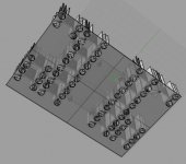
Here is an illustration just to highlight the problems one would have in routing from the DAC to the IV and from the Transistors to the output if we put hole in all the fin areas.
after the layout is done we can reapreciate it to favour puting holes below the heatsinks that most need it.....and only those.
Another issue is that the PCB might just fall apart with so many holes.")
Some holes can be omitted and size can also change according to need.
Let's see first what owen produces and the discuss this...this is my sugestion.
Here is an illustration just to highlight the problems one would have in routing from the DAC to the IV and from the Transistors to the output if we put hole in all the fin areas.
after the layout is done we can reapreciate it to favour puting holes below the heatsinks that most need it.....and only those.
Another issue is that the PCB might just fall apart with so many holes.
Attachments
Hi qusp,
you just confirmed my liking for australians, love the plave, love the people.....
Cool
, I'm glad we sorted it out painlessly, wasnt meant to cause conflictthe main reason i posted the above rendering was exactly to ilustrate where we should or should not put holes.....as it is shown it's a ver holy board....pun intended.
right, well that makes sense
but not very easy to route around as you say.
Realistically i think we should place holes only beneath the heatsink wings, this would ease the routing issue to the transistors and resistors while permiting better air flow to the heatsinks.
hmm see without some hole near the device in front of it roughly the mounting hole's height above the board in front of the part, my layout is not so clean and I have to think of whether I just leave it for the buff guys. I need to use the floor or wall for heatsinking, I cannot fit my dac + regs in the space afforded for the buff, it just wont happen. I need to mount the entire reg and dac assembly above the board, but preferably not as high as the height of heatsinks above the board.
I can mount them and then solder them in, but I would not be able to remove the IV board without destroying the sand (thats what the holes in front are for, removing the board with a screwdriver through the hole. so I guess we'll see what owen comes up with to that end.
although you could help there with your modeling software to see where the hole would have to be. thats a bit much to ask though, because if there being the heights of both to22 and to247. i'take some pics of my actual PSU tomorrow and show you what I mean. I suppose I could buy a large shallow finned flat sink from conrad and mount to that. but that would add about 100 to the build
night guys
Last edited:
Finally an update
Hi Guys,
Sorry for my absence over the past day and a bit... I've been hard at work on the layout, and trying my best not to get too distracted.
I think I've finally come up with something that will make everyone happy, and is smaller, cheaper, and doesn't require heatsinks on the board.
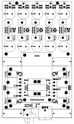
The resistors and fets are mounted between the bottom of the PCB and the bottom plate (or a heatsink if you prefer). The only on-board heatsinks are for the regs. I've upped the size of the PSU input and output caps to R18mm, and I've added an outline for the Ackodac with standoffs.
This layout will allow for either the Buffalo and the Acko DACs. It drops the board area from 50" sq to 36" sq, and generally provides a shorter circuit path for the critical connections between the DAC and I/V.
Now for the caveats:
- The Caddock resistors measure 0.127" high where the transistors measure 0.188" high. As a fun coincidence, the difference is about 0.062" which is exactly the height of normal FR4 PCB. In order to get things to clamp from the top of the board, I'll have to send shims made of old PCB material that will go between the top of the resistor, and the PCB to allow proper clamping force to be applied from the top of the board. This will be a bit of a PITA, but no more so than mounting 12 parts to board level heatsinks would be.
- The bottom of the enclosure will need to either be a heatsink, or at least a 1/4" plate to transfer heat properly. You'll need to get rid of about 42W from the DAC, excluding the regs. Bolting the parts to a flimsy 1/16" aluminum bottom will probably not be sufficient.
I've got the whole thing routed and ready to go, so all I need to do is check that my DAC fits correctly on it, and re-check the outline for the Ackodac. I still need to add tie-points for those who want to use different regs, and then I'll post the routed board up for comments on grounding and signal paths.
I'm also going to add a quad of bi-directional 2.5V zeners across each of the DAC outputs. This will prevent destruction of the DAC in the even of someone hooking things up before adjustment. It will also protect the Buffalo in the even of a catastrophic failure of the I/V circuit. With no voltage swing at the output, I doubt they will have any sonic impact. Nonetheless, you're free to not populate them if you see fit.
Any comments are welcome!
Cheers,
Owen
Hi Guys,
Sorry for my absence over the past day and a bit... I've been hard at work on the layout, and trying my best not to get too distracted.
I think I've finally come up with something that will make everyone happy, and is smaller, cheaper, and doesn't require heatsinks on the board.
The resistors and fets are mounted between the bottom of the PCB and the bottom plate (or a heatsink if you prefer). The only on-board heatsinks are for the regs. I've upped the size of the PSU input and output caps to R18mm, and I've added an outline for the Ackodac with standoffs.
This layout will allow for either the Buffalo and the Acko DACs. It drops the board area from 50" sq to 36" sq, and generally provides a shorter circuit path for the critical connections between the DAC and I/V.
Now for the caveats:
- The Caddock resistors measure 0.127" high where the transistors measure 0.188" high. As a fun coincidence, the difference is about 0.062" which is exactly the height of normal FR4 PCB. In order to get things to clamp from the top of the board, I'll have to send shims made of old PCB material that will go between the top of the resistor, and the PCB to allow proper clamping force to be applied from the top of the board. This will be a bit of a PITA, but no more so than mounting 12 parts to board level heatsinks would be.
- The bottom of the enclosure will need to either be a heatsink, or at least a 1/4" plate to transfer heat properly. You'll need to get rid of about 42W from the DAC, excluding the regs. Bolting the parts to a flimsy 1/16" aluminum bottom will probably not be sufficient.
I've got the whole thing routed and ready to go, so all I need to do is check that my DAC fits correctly on it, and re-check the outline for the Ackodac. I still need to add tie-points for those who want to use different regs, and then I'll post the routed board up for comments on grounding and signal paths.
I'm also going to add a quad of bi-directional 2.5V zeners across each of the DAC outputs. This will prevent destruction of the DAC in the even of someone hooking things up before adjustment. It will also protect the Buffalo in the even of a catastrophic failure of the I/V circuit. With no voltage swing at the output, I doubt they will have any sonic impact. Nonetheless, you're free to not populate them if you see fit.
Any comments are welcome!
Cheers,
Owen
Attachments
Forgot to mention:
CeeVee:
Those are some great renderings! I was hoping you could do me a favor and make another 3d render of the layout I just posted. It really does help to visualize things, and I am curious about the fit of the parts and any clearances my brain isn't catching in 2D
Sorry for changing everything and abandoning the previous design... I do appreciate the work you did.
qusp:
I got the ackodac stuff you sent, but I still don't know the location of the outputs relative to the edge of the PCB. If you can get me a drawing of that then I'll see if I can get the connectors to align for both boards.
There are some structural issues in CeeVee's last rendering the holes placed in line make for a delicate board . Smaller holes to screw the devices to the floor seems more feasible. Or two separate boards with devices on the sides with the option to mount separate sinks,large sinks,or case floor. Then spacing can be tweaked by each builder according to their needs. The space under the dac seems to be added real-estate in terms of board cost anyway. This option could actually give us shorter traces also. Sorry opc I didn't see your last post before submitting this the first time.
Last edited:
cool i'll have a look over that. I dont have an official spec for the placement of the outputs, but just measured it now and they are 29mm from the sides and 32mm from the 'top' they are 2mm pitch. which is a bit annoying as everything else is either 2.54 or 5.08 standard. TBH I doubt I will use a stacking headeras I need to have a layer of lexan for the regs to sit on. I will machine a hole where the outputs are so I can route wires through, but its unlikely I would use pin headers and 2mm pitch headers are not that available anyway.
most important for me are the mounting holes, you got that right? the dac is designed to have the IV stacked on it, not the other way around, but that wont work with this particular IV now will it, so I have to work with that. so I will bolt down through the lexan sheet and onto the board. sorry about no pics, had heaps on today and slipped my mind during the day as I didnt hear back.
will send pics tomorrow but its looking more workable. its a pity the linear tech regulators are more readily available, or I would suggest them as an alternative and would use the onboard supply, they are excellent and have some great HV SMD package linear regs, but yeah not all that available and at farnell where they are available, not all that cheap.
only thing is and i'm just asking your opinion here; are there some regs a bit far from the loads for low noise operation? or is the fact you are decoupling them with SMD caps making up for this? hard to see on this layout. can you have half of them on the top and the other half on the bottom?
Forgot to mention:
CeeVee:
Those are some great renderings! I was hoping you could do me a favor and make another 3d render of the layout I just posted. It really does help to visualize things, and I am curious about the fit of the parts and any clearances my brain isn't catching in 2D
Sorry for changing everything and abandoning the previous design... I do appreciate the work you did.
qusp:
I got the ackodac stuff you sent, but I still don't know the location of the outputs relative to the edge of the PCB. If you can get me a drawing of that then I'll see if I can get the connectors to align for both boards.
No i wont do you a favour opc.....it's my pleasure.
will post later...right now watching Real Madrid playing......
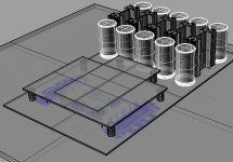
Ok game is ove and as i was multitasking i did the renders.....
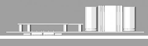
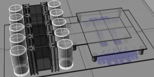
Indeed opc if you intend to pressure the caddocks and transistors against bottom of case using the pcb you will need to fill space between cadock and pcb... the other solution would be to make holes on pcb for screws to hold caddocks and transistors....anyway here are the renders for your consideration.
Bottom plate is 5mm, standoffs are 10mm and top heatsinks are 38mm high (EA-T220-38E ohmite from mouser )
Seems to me that if the DAC is Buffalo then screws should allways be placed where the ackodac's standoffs should be for better thermal contact between transistors and bottom plate of case.
Attachments
Last edited:
nice work, but the ackodac will not fit there, the regs will hit the caps. hmm the regs extend just over 50mm one way (the bottom) and 62.5 the other (the top) and out the sides, but that only matters for casing choice, the only one of consequence is most likely the top, guess we'll see
That's more or less what I was thinking... If you're using the Ackodac then the 5V reg for the DAC and the digital input section won't be any good to you. It looks like the daughter boards will still hit the caps from the other regs, but there's not much I can do about that. The Ackodac needs like 10 square feet of space around it, and there just isn't room.
I'd suggest using lower profile (1" tall) heatsinks for the regs, and lower profile caps. If you do that, you can get away with mounting the Ackodac 0.75" above the board and just wiring it in. That's still much better than some of the other I/V solutions I've seen.
If you don't use the on-board regs, then the ackodac should drop right on.
As for the distance of the regs, I don't think it'll be a problem. The output runs over a return ground plane, and each resistor has it's own large ceramic decoupling cap. PSU noise should be a non-issue in this setup.
Cheers,
Owen
yep, well as I said in the email, its not designed to be stacked on top, its designed to have something stacked on top of it. this wouldnt be a problem if the IV didnt need a square acre and 10lb of alloy to do away with the waste heat from 12 devices . for what there is there, it still takes up very little space. try using 8 PH regs on your buff and see how much space it takes up and thats effectively whats gong on here. (except these are discrete linear regs, so heatsinking isnt a problem like shunts)
but hey i'm cool with that, I may even be able to use the spare space from the vacant power supply for mounting my USB->i2s board and async reclocker. so sounds like its all covered, like I said, was a real question about the track lengths, i'm not a designer and forgot about the ground plane for the return path
. for what there is there, it still takes up very little space. try using 8 PH regs on your buff and see how much space it takes up and thats effectively whats gong on here. (except these are discrete linear regs, so heatsinking isnt a problem like shunts) but hey i'm cool with that, I may even be able to use the spare space from the vacant power supply for mounting my USB->i2s board and async reclocker. so sounds like its all covered, like I said, was a real question about the track lengths, i'm not a designer and forgot about the ground plane for the return path
Last edited:
I havent ben following ackodac since i'll be using BuffaloII but if you want , and give me the detais, i'll render the ackodac's major components in and we can have a look at what it will look like.
Edit: Ok went for a quick search and it seems that the ackodac's apendages are the issue....don't see how they can fit in.
If this board was only for Buffalo the we could even maybe fit in Salas regs. ...no qusp i'm not forgeting you, just thinking out loud.
Doing two version of the board ( one or Buffalo, one for Ackodac ) is out of the question ?
excuse the joke but making a suit that will be good for both Laurel and Hardy is ....well kinda dificult.
...I'm not telling who is Laurel and who is Hardy.
Don't get me wrong it's just that i like to try to optimize things and...opc has a dificult task here.
CV
Last edited:
I could go for a Buff-II version with Salas regs on it.
Even neater would be a Buff-II Salas reg board with 6 regs to replace the three on-board regs, the separate 5.5v reg, and the dual-reg adder board. I don't think this could be combined with the OPC D1 I/V board, but the reg board could mount on the bottom, the Buff-II above, and the OPC D1 board above.
Just a thought... I'll go with what the consensus is.
Greg in Mississippi
Good work!
I am only chiming in because of all the Buff II talk.
Just a couple comments if I may...
FWIW... I already have designed a stackable BUF-II version of a single FET per side common gate I/V PCB, but I had no idea there was any real interest in it since Legato is really IMO a better fit.
The PCB features a bone standard FET based common gate I/V with no buffer. I actually did not think there would be much if any interest in it because of the extremely high voltage/power needed to get decent results.
The voltage/power issue is one reason why I designed Legato, but the biggest reason is better performance by dramatically increasing transconductance. It uses the same common base/gate principle but produces better (measured) results with far less power and a lot less hassle.
I think the attraction to the "D1" must simply be because of the name? Nostalgia? I am honestly curious. In any case if there is enough interest I will be glad to revive the "classic" FET only PCB, and even enhance it if desired. The original was purely for my testing in development leading up to Legato.
Cheers!
Russ
Hi Guys,
CeeVee:
Thanks for the great job on the rendering, everything looks pretty good! I can send you the same basic layout info that qusp sent to me, but at this point I think good enough is just going to have to do for the Ackodac.
The acko will fit, if you omit the regs from the board, or as I said, if you mount it about 3/4" above the board and use 1" heatsinks and low profile caps. To be honest, it actually makes sense. People who bought the Acko did so because they like to tweak the regulators and supplies, so they probably won't like my "ho hum" LM based regs anyhow. I'll provide the option for off-board power supplies, and hopefully that's enough for everyone. If you think different regs will make significant difference, then you're free to use anything you like.
qusp:
Are you reasonably happy with the layout as it is? I'll post the routed images later today for a final check over.
Russ:
Could you post some measurements for the legato? I've checked your website and I don't see anything there. If you've got access to an AP I'd prefer that.
I think the interest in this particular circuit is that it's a simple, single stage/single device design with no feedback and THD performance that is so good it's unmeasurable with state of the art measurement equipment. Can you think of a reason it wouldn't be interesting? Power dissipation is the only drawback, but at 42 watts, it's a small fraction of what even a small class A amp would draw.
The legato is a two stage design with 4 active devices per branch and feedback. I'm sure it works quite well, but it's a fundamentally different circuit. I'd also be surprised if the Legato's measured THD+N was better than -112dB (measurement floor of the AP).
I like simplicity, and I like the idea of minimizing component count and circuit complexity. There's nothing special here with this circuit, I just took it a little farther than others have, and took the time to tweak the individual parts both with listening and measurements. I've posted all my results here for everyone to see, so there's no black magic or mystical claims. It's just a really good/cheap/simple circuit that performs incredibly well at the cost of a little bit of heat.
Cheers,
Owen
I havent ben following ackodac since i'll be using BuffaloII but if you want , and give me the detais, i'll render the ackodac's major components in and we can have a look at what it will look like.
Edit: Ok went for a quick search and it seems that the ackodac's apendages are the issue....don't see how they can fit in.
If this board was only for Buffalo the we could even maybe fit in Salas regs. ...no qusp i'm not forgeting you, just thinking out loud.
Doing two version of the board ( one or Buffalo, one for Ackodac ) is out of the question ?
excuse the joke but making a suit that will be good for both Laurel and Hardy is ....well kinda dificult.
...I'm not telling who is Laurel and who is Hardy.
Don't get me wrong it's just that i like to try to optimize things and...opc has a dificult task here.
CV
start talking about that kinda thing and the design as a whole will never happen, just 'dropping in' 8 discrete shunt regs is not easy, especially when some are required to be low noise 1.2v supplies. this would require an entirely new and extensive development phase. i'm not sure if you have read my posts, because there really isnt anything to sort out. i'm not using the onboard power supply, I already have power supply for everything sorted for Pierre's PCB including potted transformer etc, without this it'll fit just fine. there will not be enough people who wanted an ackodac version and yeah I have no need for it, I just want the IV and to be able to bolt the dac board to it, thats all, I wont be using the spdif, I wont be using the power supply. I would love if the power supply section could be snapped off somehow to save space for those who wont use it.
WRT buff vs ackodac, I have both; easy picking a favorite
Last edited:
- Status
- This old topic is closed. If you want to reopen this topic, contact a moderator using the "Report Post" button.
- Home
- Source & Line
- Digital Line Level
- A New Take on the Classic Pass Labs D1 with an ESS Dac