Turned out that the other dac also didn't have the reset soldered in...
It was in the corner next to big caps and didn't notice it was missing.
Strange is that the 2 dac worked differently but the problem was exactly the same. One worked for a minute, otherone shut down instantly after turn on.
It was in the corner next to big caps and didn't notice it was missing.
Strange is that the 2 dac worked differently but the problem was exactly the same. One worked for a minute, otherone shut down instantly after turn on.
Hello
Do you know if the ES9018K2M also suffers from this bug or "working condition"? or is only for the first ES9018 version?
Very thanks.
Sorry I don't have a ES9018K2M or ES9016 in hand.
If you got a well design (that means DNR and THD should be ~130dB and ~ -120dB level) DAC based on ES9018K2M or ES9016, I can help to test ^_^
BR
Paul Lu
Hi paul
How does your "default operation" occur, depend on some register setting or randomly?
How do you feed the master clock to ES9018, local 40-100MHz oscillator or sync with your source equipment?
A japanese garage audio maker "AIT lab" showed some non-harmonic spurious occurs when synchronizing clock with source, due to its jitter reduction system.
http://aitlabo.net/blog/?y=2011&m=10&d=20
upper image: without his secret timing trimming(?)
middle image:same, but 6kHz signal, that is the freq divided sampling rate with integer.(192k/32=6k)
bottom image:with his trimming
Sorry I don't have a ES9018K2M or ES9016 in hand.
If you got a well design (that means DNR and THD should be ~130dB and ~ -120dB level) DAC based on ES9018K2M or ES9016, I can help to test ^_^
BR
Paul Lu
Very thanks.
It's a PCB problem?
If not...
When I build it I ask you for support.
Regards.
Hi paul
How does your "default operation" occur, depend on some register setting or randomly?
How do you feed the master clock to ES9018, local 40-100MHz oscillator or sync with your source equipment?
A japanese garage audio maker "AIT lab" showed some non-harmonic spurious occurs when synchronizing clock with source, due to its jitter reduction system.
DAC
upper image: without his secret timing trimming(?)
middle image:same, but 6kHz signal, that is the freq divided sampling rate with integer.(192k/32=6k)
bottom image:with his trimming
Hi Shinja,
The OSC I used is crystek's CCHD950 100MHz type, I don't really know the mechanism inside of ESS DAC. The manufacturer say nothing about this.
How can the crystal synchronizing to the source? Using PLL?
Or something like: LRCK--> PLL --> 93.048MHz clock source ?
I think the bug inside of ES9018 should be related to DPLL or ASRC inside of it.
Thank you.
BR
Paul
Thank you for your reply Paul.

ES9018 can run at least 192Fs clock.
However it may not meet ESS's philosophy ,-D/A ASRCed non-bit perfect data with near perfect clock
but -D/A bit perfect data with imperfect clock (especially in SPDIF recovered clock).
But you can achieve sufficiently clean clock with jitter cleaner IC or 2nd PLL of VCXO or Li-Ta VCO.
So the bug you found seems to be the different bug AIT lab showed.The OSC I used is crystek's CCHD950 100MHz type, I don't really know the mechanism inside of ESS DAC. The manufacturer say nothing about this.
Your digital receiver (USB or SPDIF?) may be able to output 256Fs or upper clock. Simply feed it to ES9018.How can the crystal synchronizing to the source? Using PLL?
Or something like: LRCK--> PLL --> 93.048MHz clock source ?
ES9018 can run at least 192Fs clock.
However it may not meet ESS's philosophy ,-D/A ASRCed non-bit perfect data with near perfect clock
but -D/A bit perfect data with imperfect clock (especially in SPDIF recovered clock).
But you can achieve sufficiently clean clock with jitter cleaner IC or 2nd PLL of VCXO or Li-Ta VCO.
That is the same hypothesis to AIT lab.I think the bug inside of ES9018 should be related to DPLL or ASRC inside of it.
Hi Dustin,
It seems that you've not been log on diyaudio for a long time. I post my question here in case you come here again later or ...
It it no double that ES9018 has the noise bumping issue in every chip. No matter which I/V you use, discrete or OPAMP or tue (if you can done a tube output stage which can deliver ~1.5uV rms noise in audio band).
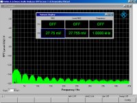
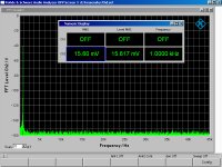
But in fact, the chip can work normally in some way. (I am not sure about the root cause and corresponding solution) Please find the measurement below:
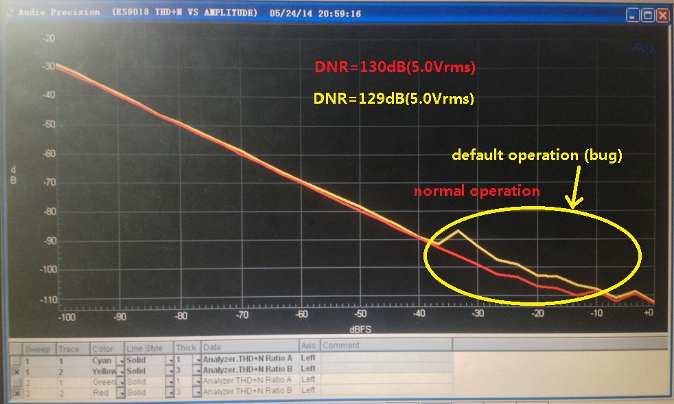
the yellow curve is the default working condition, in this way ES9018 diliver ~129dB DNR in my bench. But most important thing is that the THD+N is a little poor in the range -10dBFS to -36dBFS. When I dig it deeper, I found that the THD is not the issue, but the noise floor.
the red curve is the normal operation which I expect from ES9018. It delivers 130dB DNR and excellent THD+N in the full output range. Further check on this working condition, the whole system provide amazing linearity up to +/-1 ~2 dB error in -140dBFS to 150dBFS range.
I think all the user want to get the second operation condition from ES9018. Will you share your comment on this question?
Thank you in advance.
BR
Paul Lu
Hi Paul,
I was dealing with the same problem, thinking that it is my design's issue, until I've been told about your post.
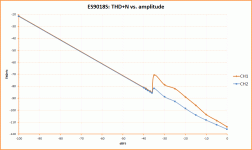
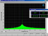
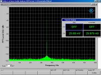
I've reached over -124dB THD and ~1.6uVrms audio band noise, which yields about 121dB DNR (my module is 8 channel with 1.6V output voltage). But interestingly, I found out that every channel has different full-scale THD+N, varying from -113 to -116.5dB. I spent tens of hours trying to solve it!
After reading your post, I sat again to R&S UPV and measured THD+N vs. amplitude and got the same result as you. There really is a bug manifesting itself between -35 and -36dBFS by steep noise rise, while THD level is not affected. However, I think it is a output, not input stage bug, because it acts differently on each channel.
Channels 2 and 6 are performing best, while 1, 7 and 8 are the worst. All measurements has been made with I2S input in asynchronous mode and the bug is present with both cheap Fox and high-quality PLEtronics MCLK oscillator.
Unfortunatelly, I can't (or at least don't know how to) make a plot of noise vs. DC level (in dBFS). Could you try to do it on your AP? I think there may be only single (or few) problematic DC level/s corresponding to certain input data levels, which could be filtered out by DSP to solve this problem.
I've sent a message to ESS tech support more than week ago... still no reply.
BR,
Pavel
Attachments
I have thought it too.
If the DAC runs differently upper/lower -36dB, it must be the cause.
but ES9018 have 64 elements, can produce ±0 to ±32 ,total 65 level ,and digital BPZ is ±0 level.
(2.112mA of offset current indicate it)
thus lower the -36dB, the DAC runs between ±0.5 level.
At that time the DAC runs like -1,0,1:2bitDAC , not 0,1:1bitDAC.
±2 level will rarely appear before -30dB.
Nevertheless the 2nd and upper DAC element/driving circuit is the cause of the noise...?
I don't have access to audio analyzer right now, but if I remember well, I measured noise with few DC offset values over -36dBFS amplitude and didn't find significant noise increase. Therefore I think this whole bug happens on one or few values.
However, now I calculated THD+N amplitude from my measured data (please see attached .xlsx) and found out that on channel 1 there is rapid increase from 1.43uV at -36dBFS to 8.35uV at -35dBFS and then decrease again with rising amplitude! I don't get it... does anybody do?
However, now I calculated THD+N amplitude from my measured data (please see attached .xlsx) and found out that on channel 1 there is rapid increase from 1.43uV at -36dBFS to 8.35uV at -35dBFS and then decrease again with rising amplitude! I don't get it... does anybody do?
Attachments
Seems like similar feature as TI DAC chips have in PCM mode, but there it is due to the combined parallel PCM & SDM and non-linearities caused by the PCM side bits kicking in. In this case, yes it is clearly 6-bit parallel output popping up, since 6-bits in binary drops out at -36 dB. Below that point is is practically multi-element 1-bit output (a bit like my DSC1 DAC is always).
Element matching is supposed to solve these issues on true multi-bit SDM (which is due to element inaccuracies), but many DACs use too simple DEM algorithm (I guess Sabre and dCS having pretty much same algo) and thus it is not completely cleaned out. In any case even when DEM is successful the inaccuracy makes SNR suffer (as it becomes white noise). I have some ideas of further tricks how to avoid SNR loss on DEM, but it is fairly complex so I doubt if such has been implemented in these low clock speed implementations. It could be done on a PC though.
In these cases, Sabre and TI are using multiple elements to boost output level at expense on distortion and linearity, probably because they cannot host high enough modulator order (MCLK ratio limiting) to have better linearity throughout. So they run out of DEM space when output becomes truly multi-bit. Using DSD with Sabre may help a little because it changes the error distribution, but since it becomes always remodulated to multi-bit SDM it cannot completely solve the issue.
However, now I calculated THD+N amplitude from my measured data (please see attached .xlsx) and found out that on channel 1 there is rapid increase from 1.43uV at -36dBFS to 8.35uV at -35dBFS and then decrease again with rising amplitude! I don't get it... does anybody do?
Low order modulators exhibit such noise modulation/idle tone behavior, especially when not adequately dithered.
..........................................................
In these cases, Sabre and TI are using multiple elements to boost output level at expense on distortion and linearity, probably because they cannot host high enough modulator order (MCLK ratio limiting) to have better linearity throughout. .....................................................
How may you appreciate the impact of an increasing MCLK ratio over the limit?
How do you see the increasing of clock frequency in such context?
I have done some experiments with higher clock frequency than the limit specified by producer. Overall results was/are positive into 125Mhz. I try to find some answers, why...
How may you appreciate the impact of an increasing MCLK ratio over the limit?
How do you see the increasing of clock frequency in such context?
It doesn't help if the DSP algorithms inside the chip are not designed to utilize higher clock speeds. And increasing the clock speed a little also doesn't yet gain more cycles per sample.
Another issue is that 100 MHz clocks tend to have at least 10 dB worse phase noise at low frequencies compared to 25 MHz ones. So from that perspective it is better to keep DSP and conversion clocks separate and asynchronous.
What I mean is that for example with a PC running at 4 GHz you have way more clock cycles per sample... And since not all algorithms can be parallelized/pipelined then the raw clock-cycles-per-sample matters (modulators are feedback control loops).
Thanks for your contribution, guys.
As far as I know, higher (than needed) MCLK frequency of Sabre DAC brings only SNR loss due to parasitic properties of both PCB, chip itself and other components. The problem we are dealing with is not caused by MCLK oscillator jitter either - as I mentioned, replacement of cheap clock by low-jitter one did not bring any improvement at all.
I measured DAC with 32 bit depth, so I don't think that introduction of dithering could make any difference.
Sabre whitepaper says in the part about HyperStream modulator:
So I assume the problem is not caused by modulator itself, unless ESS is lying there. Sygnalist, you are probably right about DEM.
My question is:
Why is the size of noise bump different on each channel? There is a 14dB bump on channel 1, but only 3.5dB on channel 2! Channel 6 is similar to 2 and others are between.
They all use the same modulator, same algorithms, same hardware. Is it possible that on-chip DAC elements are differently mismatched and DEM's effort to correct these mismatches causes different noise bumps?
If the problem was caused by modulator limit cycles, I think it's intensity would be the same on all channels.
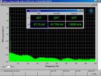
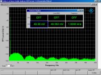
Please find attached measurements of CH1 on -25,-30,-35 and -40dBFS. I really hope someone could tell us what exactly is going on there.
As far as I know, higher (than needed) MCLK frequency of Sabre DAC brings only SNR loss due to parasitic properties of both PCB, chip itself and other components. The problem we are dealing with is not caused by MCLK oscillator jitter either - as I mentioned, replacement of cheap clock by low-jitter one did not bring any improvement at all.
Low order modulators exhibit such noise modulation/idle tone behavior, especially when not adequately dithered.
I measured DAC with 32 bit depth, so I don't think that introduction of dithering could make any difference.
Sabre whitepaper says in the part about HyperStream modulator:
The Sabre DAC shows no more than −123dB DNR even at the worst case DC offset.
So I assume the problem is not caused by modulator itself, unless ESS is lying there. Sygnalist, you are probably right about DEM.
My question is:
Why is the size of noise bump different on each channel? There is a 14dB bump on channel 1, but only 3.5dB on channel 2! Channel 6 is similar to 2 and others are between.
They all use the same modulator, same algorithms, same hardware. Is it possible that on-chip DAC elements are differently mismatched and DEM's effort to correct these mismatches causes different noise bumps?
If the problem was caused by modulator limit cycles, I think it's intensity would be the same on all channels.
Please find attached measurements of CH1 on -25,-30,-35 and -40dBFS. I really hope someone could tell us what exactly is going on there.
Attachments
Last edited:
I measured DAC with 32 bit depth, so I don't think that introduction of dithering could make any difference.
No, I meant the delta-sigma modulator dithering...
My question is:
Why is the size of noise bump different on each channel? There is a 14dB bump on channel 1, but only 3.5dB on channel 2! Channel 6 is similar to 2 and others are between.
Probably because some channels have more element mismatches than others... Or just different distribution of the mismatch vs element array.
They all use the same modulator, same algorithms, same hardware.
The analog hardware cannot be the same, the manufacturing process certainly has some tolerances.
Is it possible that on-chip DAC elements are differently mismatched and DEM's effort to correct these mismatches causes different noise bumps?
Exactly, IMO, that's where the channel-to-channel variation comes from.
If the problem was caused by modulator limit cycles, I think it's intensity would be the same on all channels.
It could still "beat" with the DEM+mismatch... So I think some of the bump could be partially coming from noise modulation that gets different whitening due to mismatches. There is always some bump?
wow it looks comb filtered noise.
Notice that the comb frequency changes as level drops. This further strengthens my belief about the element configuration they use to boost DNR.
When the level goes above -36 dB, there are more elements used in parallel and less combinations available for DEM. Quite a bit like TI/BB configuration combined with Wolfson-style element bundling.
Thank you Signalyst, seems I quite get it now...
If the noise-bumping is somehow connected to the limit cycles, then it may not appear (or appear less) with real - non-sine - music signal, am I right?
Heh, so it seems we should ask ESS for a laser trimmed or more accuratelly made chip or buy hundreds of it and make a selection.
Still, I don't get why the noise falls down again when amplitude is rising from 35dB up. There should be even less space for element scrambling...
It could still "beat" with the DEM+mismatch... So I think some of the bump could be partially coming from noise modulation that gets different whitening due to mismatches. There is always some bump?
If the noise-bumping is somehow connected to the limit cycles, then it may not appear (or appear less) with real - non-sine - music signal, am I right?
What is register 15? I just found "RESERVED, Must be set to 8b00000000 for normal operation."wow it looks comb filtered noise. I am curious what happens in other quantizer setting with register 15.
If you meant the full scale on channel 1, yes, there still can be seen that noise is shaped somehow, but it is not that clearly visible. And all other channels have noise the bump too, but smaller. On attached pictures is a comparison of CH1 and much cleaner CH2 very slightly below the bump. It's on 35kHz and on the same level relative to FS.Signalyst said:There is always some bump?
Heh, so it seems we should ask ESS for a laser trimmed or more accuratelly made chip or buy hundreds of it and make a selection.
Still, I don't get why the noise falls down again when amplitude is rising from 35dB up. There should be even less space for element scrambling...
Attachments
- Home
- Source & Line
- Digital Line Level
- ESS Sabre Reference DAC (8-channel)