I understand what you are doing there Richard the best of both things, parallel and bridged in one unit/ Seems then you would both have your power and be able to handle low impedance loads at a reasonable power level with good heat dissipation and low thd.
It turns out that since my experiments with my TDA8566 chipamp (egged on by fas42) that 'low THD' is no longer a significant target for me. The datasheet THD for the NXP TDAs is nothing special when compared to the kind of figures that LM3886 and TDA7293 chips can achieve. However the NXP's SQ is better so whilst current and voltage handling are major goals the improved THD from bridging and paralleling is just an interesting side-effect. I concentrate now on minimizing power supply noise - both from the source (whether SMPSU or trafo/rectifier/caps) and self-generated.
Paralleling does give one advantage that in theory it will allow the chips being paralleled to be spaced physically apart, hence allowing more caps to be placed closer to the chips where they have the maximum benefit. I look forward to seeing if this advantage can be achieved in practice
")
Richard that is what I understand to be distributed capacitance where you have local caps directly feeding the output devices and a main capacitor bank at the power supply. As far as fas42 I always have real problems paying attention to what he writes as is reference is some really cheap computer speakers, I can't take 90% of what he post as audio listening seriously because of this. I don't have a problem with minimizing the noise in the power supply and having good rejection but I don't think you should through out low distortion as a goal at the same time.
ps. There are way to many self powered speakers that use these chip amps and are almost universally panned as having poor overall sound quality.
ps. There are way to many self powered speakers that use these chip amps and are almost universally panned as having poor overall sound quality.
its not that I've ditched 'low distortion' just that I'm now content with 'low enough distortion' rather than consumed with adding more zeroes after the point. Because full-scale distortion is not particularly relevant, whereas low-level distortion (IMD) becomes more relevant.
Agreed that there is obviously a point of diminishing returns chasing low distortion past an already low number. Just don't want to go the other way unintentionally. As long as it is low distortion already we should try and get the noise injection from all sources as low as we can to go with the low distortion.
Right - it does seem that we do need a 'metric' to check our progress. Which is why many stick to THD, because they're unaware of any other measure in relation to audio quality. I don't have a measure at the moment so I'm rather in a no-man's land where I strive to reduce noise, without giving up on 'good enough' distortion. In the meantime I can only rely on my ears until I've developed a new measure (which I plan to do in future).
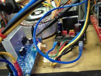
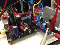
Today I tested TDA7293 buffer with LME49811 driver. TDA7293 pin 2, 3 and 4 are tied to -V rail. It has a bootstrap cap between pin 12 and 6. Pin 11 is connected to LME49811 output (SOURCE + SINK) and 7293's pin 14 is feedback point. Test circuit is shown in the picture. The circuit is working.
Attachments
Last edited:
Today I tested TDA7293 buffer with LME49811 driver. TDA7293 pin 2, 3 and 4 are tied to -V rail. It has a bootstrap cap between pin 12 and 6. Pin 11 is connected to LME49811 output (SOURCE + SINK) and 7293's pin 14 is feedback point. Test circuit is shown in the picture. The circuit is working.
HOORAY!!!
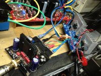
Here are the test boards for 49811 + two TDA7293 in parallel. It is working stable with 8 R dummy connected. No fault found so far. I plan to make a board for TDA7293's to measure performance. The current was purchased from TaoBao China. The layout is not good at all for measuring performance, but okay for functional test.
Attachments
I will try two TDA7293 in parallel (both slaves) and use 498xx as driver. The conceptual schematic is attached.
To assure Mute, Standby, Bootstrap all work&time identically, you might need some jumpers so the 2 slaves will function as 1.
Well, before making a new layout. I should evaluate the amp based on the existing setup. The TDA7293 board layout isn't visually bad to me (at least for TDA7293 used purely as buffer). I check distortion residual to see if there is any induction distortion (described in Self's amplifier book) due to layout or wiring issue.
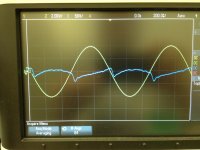
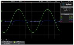
BW filter 22 Hz to 22 kHz, 8 R dummy load, 1 kHz tone, supply = +/- 25 V
THD = 0.0033 %, 10 W
THD = 0.0065 %, 1 W
Output waveform and distortion residual are shown below. To my knowledge, no sign of induction distortion is seen. Agree?
BW filter 22 Hz to 22 kHz, 8 R dummy load, 1 kHz tone, supply = +/- 25 V
THD = 0.0033 %, 10 W
THD = 0.0065 %, 1 W
Output waveform and distortion residual are shown below. To my knowledge, no sign of induction distortion is seen. Agree?
Attachments
The second thing I noticed is the input impedance to the buffer (at pin 11) isn't high. I haven't explored this much further, but I wonder if its caused by the current source from the positive supply shown in the internal schematic. About 1.5mA seems to flow from the positive supply pin (pin7) to pin11. I plan to try an equal current source to the -ve supply to mitigate this.
My measurement of current coming out from pin 11 is about 3.0 mA. Two tests were used. One connected 7293 pin 11 to ground via a 1 k resistor. Second connected 7293 pin 11 to LME49811 output (SOURCE+SINK). Two tests gave very close results. As you said, a current source from pin 11 to -V can be used to balance the current instead of sourcing from the driver stage. Is it a good idea?
Output waveform and distortion residual are shown below. To my knowledge, no sign of induction distortion is seen. Agree?
Yes, just the switching distortion from TDA7293 output...Could you load a TDA7293 output with an resistor to negative supply rail to force it a bit more to Class A? Start with ~10mA and up, until switching distortion hopefully disappear at 1W output. Watch the TDA7293 dissipation while doing it, and show as your results please.
Yes, just the switching distortion from TDA7293 output...Could you load a TDA7293 output with an resistor to negative supply rail to force it a bit more to Class A? Start with ~10mA and up, until switching distortion hopefully disappear at 1W output. Watch the TDA7293 dissipation while doing it, and show as your results please.
Thank you for your suggestion. This is similar to crossover displacement described in Self's amp book. I can try it later.
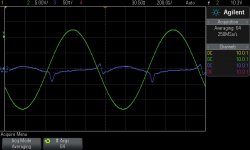
I cleaned up the wiring between 49811 driver and 7293 buffer as shown below. Distortion residual of 1 kHz, 10 W, 8 R load was checked for two ground connections of dummy load. One used the 0 V of power supply board. The other used 0 V of the amp board. To fulfill start ground, 0 V at power supply should be used. My AP did not show difference in THD (0.0033 %) of the two grounding points. Distortion residual of the right grounding is closer to "ideal" waveform - purely crossover distortion.
Attachments
Last edited:
LME49811 driver + TDA7293 buffer
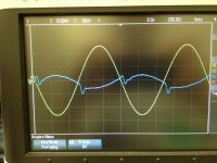
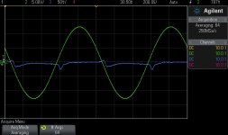
Here is result for two 7293 buffer in parallel. 1kHz, 10 W 8R THD was 0.0033 % for single 7293. It reduced to 0.0029 % for two in parallel. Not much improvement under this test condition. Distortion residual is shown below.
Here is result for two 7293 buffer in parallel. 1kHz, 10 W 8R THD was 0.0033 % for single 7293. It reduced to 0.0029 % for two in parallel. Not much improvement under this test condition. Distortion residual is shown below.
Attachments
Last edited:
Distortion residual of 1 kHz, 10 W, 8 R load was checked for two ground connections of dummy load. One used the 0 V of power supply board. The other used 0 V of the amp board. To fulfill start ground, 0 V at power supply should be used. My AP did not show difference in THD (0.0033 %) of the two grounding points. Distortion residual of the right grounding is closer to "ideal" waveform - purely crossover distortion.
As far as I can see from image, at the moment you are using one PSU with dual bridge rectification. If that is correct you should use power ground formed by local decoupling caps near TDA7293 power supply pins as your reference for signal and speaker ground reference.
I'am little suprised to see crossover distortion from TDA's even at low power level...they (invertors) claimed there will be no distortion
Crossover distortion is inevitable given the substantial mis-match in gains between the positive and negative 'sides' of the output stage. I am curious how much of the XO distortion is even harmonics? Any chance to see how the distortion residual looks in bridged mode?
<edit> Incidentally I tried playing around with loading down the output stage - this does not appear to improve the distortion as it does nothing to reduce the inherent gain mis-match between the two halves.
<edit> Incidentally I tried playing around with loading down the output stage - this does not appear to improve the distortion as it does nothing to reduce the inherent gain mis-match between the two halves.
Last edited:
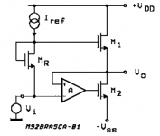
Output buffer mismatch
Here's the inner schematic from the DS - the top FET M1 is a source follower so its bound to have something less than unity gain. The M2 FET at the bottom is enhanced by the gain of the opamp.
It seems possible that a current source to the negative rail could help to raise the transconductance of the top FET but for reasonably small values of current (tens of mA) I didn't notice a significant difference. Perhaps the currents just need to be much higher.
Attachments
- Status
- This old topic is closed. If you want to reopen this topic, contact a moderator using the "Report Post" button.
- Home
- Amplifiers
- Chip Amps
- TDA7293 single, bridge, parallel