But ... if one is going to use the end result in the way an opamp is normally viewed, that is, the FB circuit defines the behaviour totally, or as close to it as possible, then the PSRR will be terribly critical. And this parameter always gets worse at higher frequencies, which is exactly where the FB has to really work hard to maintain "correct" behaviour.Bingo! That's how I figure it, too.
Dont sweat the PSRR too much if you use good, quiet multiple reg supplies and best practices in grounding.
Frank
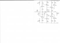
Simple circuit -100db thd and no servo needed -
Here is a really simple topology and circuit that meets my goals:
open loop bw is 25khz
open-loop h2 = -55; h3 -65
open loop gain = 62db
closed loop gain = 12db
open-loop noise (30khz bw and no wgting) = -85dbv
ref 1v into 30 Ohm load
It only uses 8 - 12 cent - transistors.
Is rock stable against dc offset changes and temp drift W/Out a dc servo appendage. And, does not have the input devices touching each other and the output does not have massive heatsinks... only individual ones. The simple diode string is not touching the output devices, either.
It can be tuned-up further. It meets my needs for a line amp. SIM the thing and let me know why you think it is so temp stable on output offset/drift. Then use what you found in your new opamp. Thx-Dick Marsh
\0
Attachments
Last edited:
... It was definitely not energy from without getting in.
And yes, when I said "light" I was speaking loosely: it was probably emission of photons near the bandgap energy at that temperature. Maybe the reason it may have gotten worse at operating temperature (~100 K iirc) is that fast electrons hitting cold lattices tend to do funny things. ...
As I recall there was an interesting pattern radiating out from the vicinity of the output amplifier. And maybe they did image it with another detector. This was all quite a while ago.
In any case, they didn't want to filter the IR outThese were custom arrays for astronomy, both for imaging with various filters in front, and for echelle spectrographs.
Bcarso
(sorry for the later reply this thread is moving fast)
Not an expert but as described to me you are correct in the fast electrons emitting photons.
I dont believe the glow was imaged with another detector but rather appearing as increased dark current around the amplifier area.
Glow appears to be dependent on the amplifier bias current, and being captured within the nearby IR sensitive array, at least for very cooled detectors.
Thanks
-Antonio
Agree. When I find the book (or the other paper) I'll confirm the account.Bcarso
(sorry for the later reply this thread is moving fast)
Not an expert but as described to me you are correct in the fast electrons emitting photons.
I dont believe the glow was imaged with another detector but rather appearing as increased dark current around the amplifier area.
Glow appears to be dependent on the amplifier bias current, and being captured within the nearby IR sensitive array, at least for very cooled detectors.
Thanks
-Antonio
Cheers,
Brad
Here is a really simple topology and circuit that meets my goals:
I like it. It is better than opamp when used as an audio amp stage.
Brad,
Re your first tests on the 2SK2145. May I suggest the following :
Assuming you use FET1 as upper FET in the follower, and FET2 as lower current source . Suggest you attach a 220R resistor between FET2 gate and FET2 Drain. FET 2 Drain connects to –Vs (I normally use -9V, but -5V also OK). You can then measure the reversed Idss of FET2 between the S & D pins. I would be interested to know how much this differs from the Idss when FET2 is connected similarly but the normal / right way round.
I am very surprised with the quoted 180nA gate current for FET1. Especially in this case FET1 is used the right way round. It sounds like FET1 is slightly forward biased. I wonder whether you still have the offset problem as you mentioned if the gate resistor for FET1 is say 100R or 1k, connected to Gnd.
I don’t think I am discouraged as yet about the follower configuration.
I shall make some measurements with a 2SK246, which is essentially the same device in TO92.
Regards,
Patrick
As mentioned there is not much offset with 2.7k to ground (an arbitrary value that was handy to use). So 100 or 1k will be similar. With a small undamped inductor (the clip lead) it oscillates, which is to be expected, indeed I'd have been disappointed if it hadn'tBrad,
Re your first tests on the 2SK2145. May I suggest the following :
Assuming you use FET1 as upper FET in the follower, and FET2 as lower current source . Suggest you attach a 220R resistor between FET2 gate and FET2 Drain. FET 2 Drain connects to –Vs (I normally use -9V, but -5V also OK). You can then measure the reversed Idss of FET2 between the S & D pins. I would be interested to know how much this differs from the Idss when FET2 is connected similarly but the normal / right way round.
I am very surprised with the quoted 180nA gate current for FET1. Especially in this case FET1 is used the right way round. It sounds like FET1 is slightly forward biased. I wonder whether you still have the offset problem as you mentioned if the gate resistor for FET1 is say 100R or 1k, connected to Gnd.
I don’t think I am discouraged as yet about the follower configuration.
I shall make some measurements with a 2SK246, which is essentially the same device in TO92.
Regards,
Patrick
.I'm fairly sure the 180nA is leakage from an isolation tub, not gate leakage per se, or a forward biased gate due to the lower "reverse-connected" FET having a higher Idss (and that at even a substantially lower voltage!). There is nothing approaching that much error with a similar configuration of the 2SK389 for example, which I have used before in the same source follower circuit with matched source load mode. Also, the large -1.48V offset was very temperature-sensitive, indicative of a leakage current and not an offset voltage as such. The pin 2 "source" voltage was being monitored all of this time with a 10M scope probe and 100MHz scope, and aside from some mains frequency hum there was no evidence of oscillations. I thought for a moment the negative offset could be due to intercepted RF, which the FET would tend to self-rectify preferentially and produce a net negative bias, with is why I a.c.-grounded the gate eventually with a small film cap with short leads. The settling time with the 8.2M R was about as expected from the time constant (270ms) upon power-up, but the final value of offset was the same.
What I have not tried yet explicitly is the common-gate loaded by the matched current load and a center-tapped floating supply (i.e., a Sen), other than that it is essentially identical to the source follower described. But as mentioned, with 2.7k in the upper base, the output offset (Sen input) gets small (I saw about 7mV), indicating the match is decent. But I can get numbers for the forward and reversed Idss of the devices individually as well, which would be interesting. There are also some parts on the way from the BL sort, the ones tested clearly having been the Y or GR based on the measured ~2.7mA.
I'm cheered that the "reversed" common-source loaded with a current source load works, with at most some slight excess leakage and good matching of currents. That by itself suggests that the reverse and forward Idss values are close, otherwise the 12k load wouldn't enough to ~center the output.
EDIT: Good news! I just reconstructed what my hookup was, as well as re-reading the statement that the tau when I added the cap was "as expected" and realizing that it was rather larger, and realized that I was bootstrapping the gate resistor of 8.2M to the source pin! Thus the equivalent source R was of order (1 - Av)^(-1) or more like 820M! That is, the equivalent R was much higher, hence the leakage current overestimated. I just went back to the setup, cleaned it up, and find that the follower offset is small. So this is very good news.
Last edited:
I realized as well that the purported 180 nA (now more like a nA) was really suspiciously large, even for a large reverse-isolation diode/ So this is a much-welcomed result.
It appears the 2145 can be used in virtually any configuration: conventional diff amp with hardwired sources, common-source with matched current gen load, common drain voltage follower with current gen source load, common-gate with current gen source load.
It appears the 2145 can be used in virtually any configuration: conventional diff amp with hardwired sources, common-source with matched current gen load, common drain voltage follower with current gen source load, common-gate with current gen source load.
I think another friend mentioned the BL, but I hope I didn't just dream itWe have difficulties getting hold of the BL grade. And we would love to do our own measurements.
If you have a source (other than Wayne) that we can obtain a few samples, please drop me a line.
More to follow...
Patrick
Yes, it would be nice to have more current. Especially now that I found my blunder!EDIT: I'll try to do a better measurement of Ig after some more sleep. I could infer it by guessing at what the 10M-loaded follower gain is and hence what the effective laod R was, but a more direct measurement with a high-meg R is also possible with some attention given to shielding. I'll bet it is a good deal less than a nA (which is the max spec for the conventional hookup).
Last edited:
> Especially now that I found my blunder!
So at least we can still trust Toshiba quality.
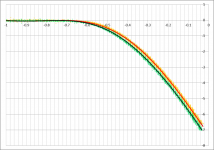
Below our own measurments of a Toshiba 2SK3320GR, same device but smaller package.
Red line = FET1 DS-reversed
Orange X = FET1 DS-proper
Black line = FET2 DS-reversed
Green X = FET2 DS-proper
X-axis is Vgs in V, Y-axis is -Id in mA.
So as one can see, decent matches between FET 1&2.
And no measureable differences with reversed Drain-Source.
More measurements to come in the next weeks....
XEN Audio at your servive.
Patrick
So at least we can still trust Toshiba quality.Below our own measurments of a Toshiba 2SK3320GR, same device but smaller package.
Red line = FET1 DS-reversed
Orange X = FET1 DS-proper
Black line = FET2 DS-reversed
Green X = FET2 DS-proper
X-axis is Vgs in V, Y-axis is -Id in mA.
So as one can see, decent matches between FET 1&2.
And no measureable differences with reversed Drain-Source.
More measurements to come in the next weeks....
XEN Audio at your servive.
Patrick
Attachments
Last edited:
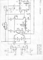
I used Google to translate the website I linked in an earlier post :
http://www.diyaudio.com/forums/anal...discrete-opamp-open-design-9.html#post3143146
As you can see the topology is essentially identical to the "Constellation" circuit John posted here first.
This particular topology is known as the Kaneda topology and is extremely popular. You can find hundreds of DIY projects from IV converters, preamps, power amps, .... based on the same. The first circuit was supposedly published in 1973 by Professor Akihiko Kaneda. I guess in those days the rest of the world was not paying much attention to Japanese audio design.
I post the translation here for your interest. The author also has a few interesting device choices.
Patrick
Attachments
> Especially now that I found my blunder!
Below our own measurments of a Toshiba 2SK3320GR, same device but smaller package.
Red line = FET1 DS-reversed
Orange X = FET1 DS-proper
Black line = FET2 DS-reversed
Green X = FET2 DS-proper
So as one can see, decent matches between FET 1&2.
And no measureable differences with reversed Drain-Source.
More measurements to come in the next weeks....
XEN Audio at your servive.
Patrick
Could you also measure the two on resistances, forward and reversed? I don't think that was an artifact of my setup, but it is not impossible.
But we would expect near-symmetry, as observed, unless something strange was going on. Also, despite the relatively small Idss, according to the datasheet the gm should still be high enough at that Idss to give of order 1nV/sqrtHz (based on the first-order theory of the equivalent noise resistance being 0.67/gm).
Yes, except for the rather limited power dissipation, I think these parts can be quite versatile indeed.
> Could you also measure the two on resistances, forward and reversed?
Not possible in our current setup.
And we don't intend to use it as a switch.
We specialised in customised heat sinks.
So abit of dissipation does not really worry us.
Patrick
Well the nice thing about typical SOT-packaged JFETs is that the gate lead is what the chip sits on, so despite the small size it is possible to do fairly effective heat sinking. If in fact (as a friend speculates) the 2145 may be actually two isolated chips before the common-source connection, maybe it too has each chip on a gate lead. I wish I had an x-ray machine handy.
And yes the parts mentioned are BL, I went back and found the email.
Now to sleep, perchance to dream
First, I did not disparage the numbers as unrealistic.Case 1 (Silicon mass temperature at t0: Ts0=20C)is for a typical case of an IC in ambient temperature.
Case 2: (Silicon mass temperature at t0: Ts0=40C)is for the case of an IC intentionally control heated.
If you think that Ta=100C and Tb=70C are unrealistic, please put reasonable numbers.
OK, lets assign a thermal resistance between the chip bottom and the transistors. For a transistor 10 mils by 10 mils and 15 mils thick, the equation is: (note, math aint my strong point, let me know if anybody sees errors..
(linear distances in inches)
R = thickness/(K times area) degrees C per watt. (k for silicon, 3.3)
R = .015/(3.3 times .01 * .01
R = 1.5 10e-2/( 3.3 * 10e-2 * 10e-2)
R = (1.5/3.3) 10e+2, or... 45 degrees c per watt.
Your case 1:
base at 20, T1 at 100, 80 degrees rise, dissipation needed: 80/45, 1.77 watts.
T2 at 70, rise of 50, dissipation required: 50/45, or 1.1 watts.
case 2.
base at 40:
T1 60 degree rise, 1.5 watts dissipation.
T2 30 degree rise, .66 watts dissipation.
Summary,
case 1 the chips dissipate 1.77 watts and 1.1 watts, a ratio of 1.6.
case 2, the chips dissipate 1.5 watts and .66 watts a ratio of 2.2.
Your thinking is flawed only in that you are setting the chip temperatures without regard to the dissipation required to do so.
I had to stay away from beer for 5 years after a stomach operation. (I was told that after the operation
Now I drink again, not a lot but I enjoy it.
George
It's amazing what you miss when it is unavailable to you.
I miss my mind the most..
jn
Here is a really simple topology and circuit that meets my goals:
\0
Except it's not an op-amp and not an easy drop in in lots of places. Does not scale easily to phono use either.
Except it's not an op-amp and not an easy drop in in lots of places. Does not scale easily to phono use either.
However it is nice to have universal building blocks, but for critical applications specialized solutions will be always better.
- Home
- Source & Line
- Analog Line Level
- Discrete Opamp Open Design