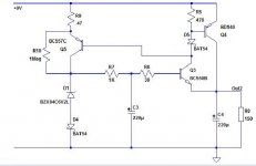
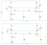
I made schematic of a Zener follower after reading post from Alciad
http://www.diyaudio.com/forums/chip-amps/49619-opa549-gainclone-layout-8.html#post587354
I am not sure if my design is correct. I used BF862 as current source in my schematic. J511 is FET current source and hard to source.
Please help me out by correcting this schematic.
Why would you waste your time and parts with something so poor?
The output is anything but regulated, both versus input and load variations, and temperature sensitive as well ( very much so ).
LM317 and LM337 with a 10uF at the adj pin for better ripple rejection, and 47-100uF at the output for stability reasons, is all you need, and it's performance is way better ( and also it's much simpler than that nonsense ).
High-end is not about overkill. High-end is not about over-complicated circuits. High end is not about unrealistic specifications >60dB better than audible. High end is about good measurable performance and no objections from the "reptile" corner of human senses, that can inspect matter down to sub-atomic quantum physics signatures, and can do heuristic computations to determine if something fair or nasty is going on inside equipment or organisms. High end can be achieved in many ways, and surely by the wise use of integrated circuits. My field of investigation is switching mode and mixed signal audio electronics, like class D, SMPS and MCU embedded into audio amplifier, these are among the biggest challenges in high-end audio electronics, so I have enough background to make that affirmation about ICs.
Elvee,sorry to bug you too much. How can I make your design to a Bipolar one?To improve the line regulation, you can use this simplistic fix: just replace the jFET CCS with a banal BJT CCS, and you gain 40dB of static line regulation.
The higher frequency behavior remains unchanged because ultimately it is dictated by the Early effect of the transistors.
Note that this mod will also greatly improve the load regulation.
R10 is required to make the circuit start by itself, but it degrades the performances only very slightly
Too complex for me to change things around
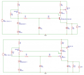
Elvee,this is a very basic question , your circuit posted in #21 The out put will be +6V and Zero or is it 6V and Zero? The reason why I asked is there is some difference in Transistors arranged in my original circuit to get + 6 V. My design was faulty to begin with?i was using BC550 and BD139 to get the positive rail.BC560 and BD140 for negative. You are using BC550 and BD140 for the circuit. Since. Don't know much about the design thought I would ask.
Last edited:
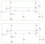
If in may, instead of two transistors of the same polarity here is a PNP/NPN combination.The purpose is to loose as little as possible from the small difference from 9 to 6 volts for the transistors to work with.Elvee,this is a very basic question , your circuit posted in #21 The out put will be +6V and Zero or is it 6V and Zero? The reason why I asked is there is some difference in Transistors arranged in my original circuit to get + 6 V. My design was faulty to begin with?i was using BC550 and BD139 to get the positive rail.BC560 and BD140 for negative. You are using BC550 and BD140 for the circuit. Since. Don't know much about the design thought I would ask.
There is still a (very) little gain (voltage wise) in using a schottky for D5.
Mona
Attachments
Attachments
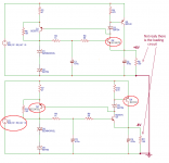
Rectifichanges ?Mona , what are the circles over the transistors means?

Mona
- Status
- This old topic is closed. If you want to reopen this topic, contact a moderator using the "Report Post" button.
- Home
- Amplifiers
- Power Supplies
- Zener+Voltage follower