Hi Grataku,
No, but is similar to something I am working on. I have used j-fets in my design to avoid the input coupling capacitors. I think this might be a good starting point towards the next Zen.
You are correct, I would use emitter resistors for the outputs.
Regards,
Jam
No, but is similar to something I am working on. I have used j-fets in my design to avoid the input coupling capacitors. I think this might be a good starting point towards the next Zen.
You are correct, I would use emitter resistors for the outputs.
Regards,
Jam
You don't think I was going stay out of it......
Put a cap across the series combination of R3 and R13 and take the input cap to the gate resistor of one of the mosfets. Power supply noise will modulate the bias current for the mosfets and show up as part of the input signal. The gate to source voltage is pretty sure to be different for the 610 and 9610 mosfets even with the same bias current through them. You probably want to put a pot as part of the resistance of both R10 and R11 as you will need to adjust the gate to source voltage across R3 and R13 (which can be one resistor now) you will never get a stable bias current for the output stage without some degeneration. I would be looking at 1 ohm and 0.5 ohm at the very least. Your DC offset is still going to move to a great deal I fear since the negative feedback is DC coupled as well as the bias and DC offset moving with power supply changes (and they will move as the line voltage does. It is probably a workable topology if you pay attention to these concerns. Of course, I gladly submit to any veto power that Mr. Pass might exercise. It is actually has the potential for a good amplifier in my first estimation. I might shoot for 30 volt rails and an amp of bias for the output stage. I will definitely simulate it and might build one if the Spice results look reasonable for stability and open loop gain.
Put a cap across the series combination of R3 and R13 and take the input cap to the gate resistor of one of the mosfets. Power supply noise will modulate the bias current for the mosfets and show up as part of the input signal. The gate to source voltage is pretty sure to be different for the 610 and 9610 mosfets even with the same bias current through them. You probably want to put a pot as part of the resistance of both R10 and R11 as you will need to adjust the gate to source voltage across R3 and R13 (which can be one resistor now) you will never get a stable bias current for the output stage without some degeneration. I would be looking at 1 ohm and 0.5 ohm at the very least. Your DC offset is still going to move to a great deal I fear since the negative feedback is DC coupled as well as the bias and DC offset moving with power supply changes (and they will move as the line voltage does. It is probably a workable topology if you pay attention to these concerns. Of course, I gladly submit to any veto power that Mr. Pass might exercise. It is actually has the potential for a good amplifier in my first estimation. I might shoot for 30 volt rails and an amp of bias for the output stage. I will definitely simulate it and might build one if the Spice results look reasonable for stability and open loop gain.
You don't think I was going stay out of it......

and post results for us?Fred Dieckmann said:
I will definitely simulate it,
Fred,
Maybe we need to take this design to the next level. I like your ideas and maybe double up the output stage ( with suggested source/emitter resistors ).
I will post my design as soon as I get it working.
Pedro,
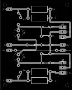
Nice, clean layout. The only thing I would do different would be to thicken the B+, B- and output traces. ( How about local decoupling caps for the B+ and B- rails)
Peter,
It is time to get off the gain clone kick.......and build a real amplifier.
Regards,
Jam
Maybe we need to take this design to the next level. I like your ideas and maybe double up the output stage ( with suggested source/emitter resistors ).
I will post my design as soon as I get it working.
Pedro,
Nice, clean layout. The only thing I would do different would be to thicken the B+, B- and output traces. ( How about local decoupling caps for the B+ and B- rails)
Peter,
It is time to get off the gain clone kick.......and build a real amplifier.
Regards,
Jam
jam said:How about local decoupling caps for the B+ and B- rails
[/B]
what do you mean by that?
 please sketch your idea. I'm not an expert on this matters.
I allready made some track thickness changes to 3.0mm. Is this ok?
jam said:Pedro,
I ment to add some capacitors about , say 100uf, between the supply rails and ground, close to the mosfets and ground. I would make the tracks as thick as possible.
Regards,
Jam
sorry about the question, but what is the purpose of those caps?
they aren't at NP design, are they?
Got the parts and the boards are allready made
I'll start building the amp in the weekend.
Just need a few more help, here goes:
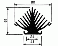
1- do the mosfets of PSu need dissipation? how much of sink' is needed?
2- what is the "amount" of heatsinks required for a 25V trafo's and 2A bias? I ussually measure heatsinks in kg (hehehe).
for ex: in 5W soz I used 4kg/ch
in Aleph 5 I used 7kg/ch
both are working at +- 50ºC
What is your estimate for this one?
I'll start building the amp in the weekend.
Just need a few more help, here goes:
1- do the mosfets of PSu need dissipation? how much of sink' is needed?
2- what is the "amount" of heatsinks required for a 25V trafo's and 2A bias? I ussually measure heatsinks in kg (hehehe).
for ex: in 5W soz I used 4kg/ch
in Aleph 5 I used 7kg/ch
both are working at +- 50ºC
What is your estimate for this one?
Hi everybody...
wouldn't it be useful to separate the PSU of the MOSFETs and the input resistors? I mean lot of PSU noise comes from that fact that the reference is the power rail - as mentioned in Nelson's article - not the ground. If you take the smallest transformator with some regulation used exclusively for the resistor ladder fomed by R3 and R4 you could eliminate most of the nosie very effectively. It is otherwise a very hard task because of the high currents...
Or not?
cheers
bt
- Status
- This old topic is closed. If you want to reopen this topic, contact a moderator using the "Report Post" button.
- Home
- Amplifiers
- Pass Labs
- Zen Variations 5