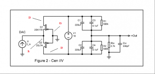
> I do have some dc offset in the output of one channel. Whats the best way around this, trimmers in series with the 560k resistors?
You should trim the output DC by adjusting the current source that you added according to post #301.
You are obviously not compensating exactly the 2mA (whatever the exact value and may also vary from chip to chip) current sink of the TDA1541.
You should measure both input and output DC while trimming.
Changing R1, R2 will not solve your DC out problem.
Maybe QSerraTico_Tico can give you more advice.
I do not have a TDA1541 to play with, so I cannot tell you exactly how it behaves.
Patrick
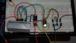
I made a try, breadboarding it.
I used what i got in hand, matched jfet at about 7.5mA and 1.5k Riv, NiMh DC 18V battery, electrolytic and wima cap, the I/V was behing an AD1865.

Is there any mistake ?
I got offset at input (10 DC mV to DAC ground) and output (30mV). I got sound but a little distorted... A "pseudo" simple thermal coupling (using UGS heatsink) was used but not enough i think...
I used what i got in hand, matched jfet at about 7.5mA and 1.5k Riv, NiMh DC 18V battery, electrolytic and wima cap, the I/V was behing an AD1865.

Is there any mistake ?
I got offset at input (10 DC mV to DAC ground) and output (30mV). I got sound but a little distorted... A "pseudo" simple thermal coupling (using UGS heatsink) was used but not enough i think...
Nothing wrong that I can see.
The input DC is due to JFET Idss mismatch.
A better matched pair plus better thermal coupling will cure that.
But the DAC will still work with 10mV.
The output DC might be from the DAC itself (leakage of 20uA at no signal).
Try measuring it again with the input open (no connection to DAC).
As to distorted sound (never happened to us), first check output with no input connected (open, no DAC).
If you see oscillation, you can add 2x 100R gate stoppers between Gnd and JFET gates.
Then feed your DAC with a 1kHz digital signal (-6dB from full scale) and measure the output with an oscilloscope.
We'll then take it from there.
Patrick
One of you mailed me about drift problems of the JFET current source used to counter-bias the TDA1541.
Apparently the sound was very good when DC was under control, to justify further experimentation.
JFETs wired as current sources, even with degeneration, are very sensitive to temperature and hence drift. You may consider using a degenerated BJT, such as BC560C, biased by a voltage reference (e.g. a Zener or chain of LEDs), instead. Or even simply a regulated power supply (say +12V) and a resistor (6k nominal, trim to zero DC).
Perhaps others who have used TDA1541 has proven solutions ?
Patrick
.
Last edited:
Dear All,
I am going to assemble the bjt circuit posted in post #6s by Calvin. I have few questions:
1) I see there power supplies, one 12V and two 9V. Do they all need to float ?
2) Is the value of the 1k45 resistor critical ? I found this resistor only in SMD. I could use 1k5R.
3)How do I have to match the BJT, and how close they have to be ?
This will be tested with an AD1865 chip.
Thanks,
Davide
Calvin can probably give you more definitive advices, but I'll give it a try.
1) 12V needs to float. The two 9V are +/-9V referenced to DAC Gnd, so not floating.
(You might get away with just using the 12V by using constant current diodes to replace R1, R2 in his schematics, and tie them to both ends of the 12V. But I have not tried.)
2) Not critical. They set the bias of the circuit. I would use 1k2 or even 1k for AD1865.
3) I normally match to 0.5% hfe or better. But Calvin probably has more experience with current mirrors.
Patrick
Hi,
1) just V1 needs to be floating. V2 and V3 are symmetrical voltage gnd referenced supplies. If You don´t use a buffer following the I/V resistor then I´d suggest to use just one floating supply and JFETs, simply because of practicality reasons.
2) The value of R1 and R2 is non critical. It sets the idle current in the Input transistors Q1 and Q2. 1k5 instead of 1k45 reduces the idle current from 5.mA to 5.7mA. The idle currents affect distortion values and to a certain degree noise. Values around 4-8mA are ok for the simmed transistors. THD figure sinks a bit with rising I-idle, with the phenomen that K3 almost remains constant and only K2 varies. With I-idle below ~5mA K2 is dominant, above ~6mA K3 becomes dominant.
You may rise V1 to 18V (2x9V battery) and set R1, R2 to 1k5 to 2k (5.8mA - 4.4mA). Heat dissipation of Q1, Q2 remains below 55mW (18V/5.8MA) which is low enough for the SMD-transistors. Feeding +-1mApp from a AD1865 and using a Riv of 2k2 and R1,R2=2k sims a Vout of 1.5Vrms and THD -111.28dB, K2: -112.dB K3: -118.9dB). R1,R2=1k5 gives THD -114.8dB, K2: -116.3dB, K3: -120.2dB.
3) Taking transistors from one batch and couple well thermally should already give low enough offset. The coupled emitters of q1, Q2 tend to cancel out mismatches between Q1/Q3 and Q2/Q4. But I´d use dual-transistors. There are several manufacturers for duals of the 546/547/550 --557/559/560 and the cost difference is so low that it is sensible to not undergo the effort of matching devices.
Sourcing these duals should be no big problem.
Or use the SMD-Duals of the simulation file from Diodes/Zetex or Philips.
regarding the drift problem of the JFET-CCS: Yes, the simple CCS reacts on temperature, but it is the lowest noise CCS I could find. Since this CCS is connected to the Input of the I/V stage, all noise is transferred to the output. In fact the CCS may easily be the dominant noise source of the hole circuitry. Bipolardualtransistortemperaturecompensated, integratedlownoisespeccedCCS all were considerably noisier than the simple oneJFEToneResistorCCS. So its probabely best to let the circuit heat up to its working temperature to null out offset and to thermally shield/encapsulate the CCS and I/V stage in a closed casing.
jauu
Calvin
As to distorted sound (never happened to us), first check output with no input connected (open, no DAC).
If you see oscillation, you can add 2x 100R gate stoppers between Gnd and JFET gates.
Distorsion vanished with the 2x100R gate stoppers... Amazing
I quickly compare it to Spencer D1 jfet I/V (also 2sk170/sj74, R Vishay Bulk metal foil, PIO coupling cap) for the left channel, CEN using basic material for the right.
Comparison was made with CD having the same mono sound on both channel.
Sound was great in both case, for sure really better than opamp IV. I cannot tell whether Spencer D1 or CEN is better... They are closed... CEN is opened to simple improvement (Better RiV...) and should be better as my try is really not optimized (see picture)...
One default
So really, thx Patrick for sharing

PS : Have you compared CEN/SEN to one of your previous concept http://www.diyaudio.com/forums/digital-source/168093-hawksford-discrete-iv-twist.html
Last edited:
Thanks for reporting the results.
You should do the circuit some justice by using proper PCBs, etc.
The PCB for the GB has already allowed for the gate stoppers.
So you did have oscillation.
You can use rechargable batteries and use a relay to switch it to charge as you switch off the player.
We do exactly that.
As to other circuits.
We have our own version of all.JFET D1, and the Hawsford as you mentioned.
They do not offer any sonic advantages but are much more complicated.
And the CEN / SEN are dead quiet !!!
As said, we use SEN ourselves for PCM1704.
Patrick
Hi,
tested the Hawksford after thê C111-article, Fig 4.4.
While it sounded better than a OP-IV it was no better than a improved Jocko, which is still my personal favourite for DAC-chips with an offset current output, because of the simplicity of the circuit (1x JFET-CCS and 1x biolar Dual + output Buffer stage).
There remained a certain grainyness in the sonic character of the Hawksford-circuit that I know so well from globally fed-back circuits. Regardless of featuring error-correction the distortion was not as low as I´d expect from a feedback circuit, hardly better than -70dB@0dBfs.
The optimized Jocko shows much less THD at better -90dB@0dBfs (2.1Vrms from a +-2mApp Input). Further improvements in THD are rather an academic than a sonic issue.
jauu
Calvin
The Hawsford variant that I published has some improvements over the original.
And it has a lot more driving capabilities (e.g. for a low impedance headamp).
But I agree that the error correction does not deliver the promised sonic advantage.
And the CEN/SEN are really hard to beat for its own intrinsic distortions.
We have some ideas how to improve the SEN further.
But work in progress, and not ready for publication for another 6 months or so.
Patrick
Guess this is what Calvin was referring to :
http://www.diyaudio.com/forums/digital-source/6121-easy-build-i-v-stage.html
Patrick
http://www.diyaudio.com/forums/digital-source/6121-easy-build-i-v-stage.html
Patrick
- Home
- Source & Line
- Digital Line Level
- Zen -> Cen -> Sen, evolution of a minimalistic IV Converter