revised amp schematic with beefier drivers
Here is the revised schematic.
-- Added more driving punch between the si824x and the output stage, to support big fat mosfets (thanks luka and smms73).
-- added Zobel networks (thanks Ouroboros)
-- corrected a mistake (D2, D3, D7 and D8 were in the wrong place at the wrong time, thanks Ouroboros)
-- re-arranged the drawing
Enjoy while you can, because I'll soon move on to the protection circuitry.
E
Attachments
Last edited:
That would be a good idea, to keep both threads focused.Elevator if you want, you can open another thread to discuss the eGaN FETs.
Your contributions are much appreciated.
E
Your contributions are much appreciated.
E
Thanks.
you need to use a snubber between the drain and source of the output mosfets, a resistor of 10 ohm in serie with a capacitor of 220p should be good, this serves to dump some of the ringing of the output cause by the infamous parasitic inductance's
PS- and if you want, put a resistor between the pin 5 and 4 of the zxgd3002, if you do that, the si8244 can help to drive the mosfets a resistor of 1 ohm should be good.
Last edited:
Pd, confused...
To follow up on an earlier discussion about maximim allowable Ciss for the Si824x chip, I'm having trouble getting the Pd calculated as per the Si824x datasheet. Pages 18-19. Maybe I'm just thick.
The chip is limited to ~1.2W dissipated power. This in turn limits the max allowable load capacitance CL (~the mosfet Ciss) at a given frequency.
According to the upper graph on page 19, at 500kHz CLmax is about 2.5nF before the chip overdissipates.
I went back to calculate the power dissipation for our design using equation 1 on page 18. As a result, I see that max dissipation is reached with a CL of around 7.5nF. Spreadsheet is attached.
Why is this important? Because in view of the 2.5nF limit, it was decided to add another driver stage after the Si824x to allow driving big-fat mosfets, i.e representing a CL >> 2.5nF.
If however the real limit is found to be 7.5nF, the case for an additional driver would arguably become much weaker IMO.
My suspicion is that the graph on page 19 assumes a much higher Vddo than our VGD=12V. Remember Pd goes with Vsquared.
Plugging in Vddo=20V in my worksheet for eq.1 does indeed yield Pd(max) with CL~2.5nF. Also, on page 18, assumptions for Eq. 3 and 4 are Vddo=18V...
Can somebody re-check this?
Because I may have screwed up again
E
Attachments
Last edited:
I'm not sure I entirely understand this.Thanks.
PS- and if you want, put a resistor between the pin 5 and 4 of the zxgd3002, if you do that, the si8244 can help to drive the mosfets a resistor of 1 ohm should be good.
Sinking would be ok, the 824x helping through the 1 ohm resistor. But how does it pull the line back up over the threshold? It seems that it is stuck low, fighting with the ZX sink output which may have an RDSon considerably lower than that of the 824x source plus 1ohm...
So if there's a fight, power would be wasted...
E
I'm not sure I entirely understand this.
Sinking would be ok, the 824x helping through the 1 ohm resistor. But how does it pull the line back up over the threshold? It seems that it is stuck low, fighting with the ZX sink output which may have an RDSon considerably lower than that of the 824x source plus 1ohm...
So if there's a fight, power would be wasted...
E
No, there is no fight, because the si8244 controls the zx, the pnp transistor of the zx just turn on when is more than 0.6v across the 1ohm resistor (0.6 amperes ) to help out the si8244, the real problem is that the si8244 when sinking would saturate the pnp transistor . So now, i don't think is a good idea.
I can not check your calculations right now, but i think you are right, 2.5nf is to low.My suspicion is that the graph on page 19 assumes a much higher Vddo than our VGD=12V. Remember Pd goes with Vsquared.
Plugging in Vddo=20V in my worksheet for eq.1 does indeed yield Pd(max) with CL~2.5nF. Also, on page 18, assumptions for Eq. 3 and 4 are Vddo=18V...
Can somebody re-check this?
E
Its a bit overkill to use the ZX . you be better without them.
Last edited:
revised amp schematic, corrected mistakes
Although the last few days I have been busy with the fantastic Uber module, the Silabs-based amp is not forgotten.
Here is the latest version of the signal path schematic which corrects a few mistakes
- changed the VGD regulator transistor to a darlington (any halfway decent darlington will do)
- same subcircuit, added cap parallel to zener
- idem, higher value for R12
- added snubber networks to the output fets
The above are all thanks to smms73.
After this has been digested, I will finally move on to the protection circuitry...
E
Attachments
With my bridged UCD designs, I use balanced feedback for the (separate) self-oscillation path signal and the audio output signal. With your design it would easily be possible to provide balanced feedback into U1b. You could get it running with feedback from one half of the bridge first, then modify it to provide full differential feedback and see if the performance is better.
is it ok to take the feedback only from one branch of the bridge?
In principle it is ok to take one arm only - if all else works, the other is just the complementOuroboros: I use balanced feedback for the (separate) self-oscillation path signal and the audio output signal. With your design it would easily be possible to provide balanced feedback into U1b. You could get it running with feedback from one half of the bridge first, then modify it to provide full differential feedback and see if the performance is better.
But I thought about at least providing the hooks for balanced feedback from the oscillation path. Not sure what it would bring, but worth trying out. I am much less convinced by feedback from the audio path, ie after the LC and Zobel. That's a possible can of worms IMO.Thanks for the feedback
,E
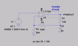
Hi Andrew,Hi all -- could someone explain how this design "self oscillates" such that the comparator does not require a triangle wave input? I don't understand how the pwm signal is being generated in this design.
It's self-oscillating. An amplifying oscillator, or an oscillating amplifier
Here's an Ltspice bone-level schematic to show the principle.Cheers,
E
Attachments
- Status
- This old topic is closed. If you want to reopen this topic, contact a moderator using the "Report Post" button.
- Home
- Amplifiers
- Class D
- YAUSA - Yet Another Ucd (S?) Amp with SiLabs Chip