andy_c said:Proposed solution?
Do it the traditional way and limit the VAS output current.
Regards,
Edmond.
andy_c said:LOL! I got tired of the Andy Singer avatar and put Dr. Diamond there instead.
Those avatars can confuse people. Here is a message I got recently
"Dear Glen,
congratulation for your projects in your site. I would like also to tell you that you are so beautiful.
But I am not writing you for this reasons, even if it would not be a bad idea............"
Cheers,
Glen
2nd reply
Hi Andy,
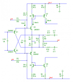
Using +/- 90V rails, this version consumes far less power in the resistors that act as a CCS (R1...R4), although the currents through R6,7,9,10 are still rather high at full output power. Increasing the resistor value not only decreases the bias current (no problem, just increase V5), but also lowers the current feedback, which we don't want.
Perhaps you wonder why increasing the gain of the OPS anyhow? As mentioned elsewhere, for two reasons:
1. A better step response, no overshoot neither peaking at about 3MHz.
2. Lower supply voltages for the front-end and 'headroom' for voltage regulators.
But at the expense of wasting power in the gain setting/feedback resistors (R6..10). As you see, there is no free lunch.
As for that 'small resistor', now I see what you mean. It's R19, right? Indeed, one can up the bias current with R19, but, as said before increasing V5 does the same job.
One more thing: I feel uncomfortable with the high power dissipation in Q7 and Q8. Why not using simple 1:1 current mirrors and adding an extra class AB EF stage before the drivers? And, perhaps even more important, you can use the emitters of this stage as the take off point for the frequency compensation. In this way you have sufficient gain (one beta) inside the compensation loop. Opposed to YAP, this paves the way to a more sophisticated compensation scheme, TMC or TPC for example.
See also: http://www.diyaudio.com/forums/showthread.php?postid=1613482#post1613482
Regards,
Edmond.
andy_c said:Well, I'm looking at +/- 90V rails, so that ends up being lots of current through the feedback loop at max output power. It seems like increasing R6, R7, R9 and R10 to keep that current down would then constrain the input stage bias current to be pretty low.
Edit: Scratch that
I see what you're saying, though. That's a cool way of bootstrapping using only resistors.
Hi Andy,
Using +/- 90V rails, this version consumes far less power in the resistors that act as a CCS (R1...R4), although the currents through R6,7,9,10 are still rather high at full output power. Increasing the resistor value not only decreases the bias current (no problem, just increase V5), but also lowers the current feedback, which we don't want.
Perhaps you wonder why increasing the gain of the OPS anyhow? As mentioned elsewhere, for two reasons:
1. A better step response, no overshoot neither peaking at about 3MHz.
2. Lower supply voltages for the front-end and 'headroom' for voltage regulators.
But at the expense of wasting power in the gain setting/feedback resistors (R6..10). As you see, there is no free lunch.
As for that 'small resistor', now I see what you mean. It's R19, right? Indeed, one can up the bias current with R19, but, as said before increasing V5 does the same job.
One more thing: I feel uncomfortable with the high power dissipation in Q7 and Q8. Why not using simple 1:1 current mirrors and adding an extra class AB EF stage before the drivers? And, perhaps even more important, you can use the emitters of this stage as the take off point for the frequency compensation. In this way you have sufficient gain (one beta) inside the compensation loop. Opposed to YAP, this paves the way to a more sophisticated compensation scheme, TMC or TPC for example.
See also: http://www.diyaudio.com/forums/showthread.php?postid=1613482#post1613482
Regards,
Edmond.
Attachments
quote
LOL! Somebody over at Audio Asylum recently referred to "Sound By Singer" as "Sound By Sphincter"
Sounds about right.
Time to come down to earth and sell $5k amps and not the $30k jobs he touts normally, especially now tha t all his banker clients have flown south for the winter
LOL! Somebody over at Audio Asylum recently referred to "Sound By Singer" as "Sound By Sphincter"
Sounds about right.
Time to come down to earth and sell $5k amps and not the $30k jobs he touts normally, especially now tha t all his banker clients have flown south for the winter
Re: 2nd reply
I had looked at this briefly in the past and had oscillations. I was also having other problems at the time, so I didn't pursue it further back then. Since things were more stable now (or so I thought), I decided to revisit the predriver idea.
I did indeed see oscillations again when the predriver was added, and tracked it down to a local Miller loop instability. I was initially able to get it barely stable by putting base resistors in the CB stage of the Hawksford cascode, and based on this data, I found that under high-slew conditions, the total peak base currents into the predriver were about half of those into the driver. Not as much of an improvement as I would have hoped, but it gave hope for reducing the "VAS" current from 30 mA to 10 mA, which would then allow replacing the 2SC4793/2SA1837 cascode transistors with KSA1381/KSC3503. I also got a slight reduction in distortion, presumably due to lighter loading on the "VAS".
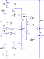
This led to the need for analyzing the local Miller loop gain. With non-complementary circuits, I have always done this by blocking the global feedback (for all but DC) by putting a huge series inductor and shunt capacitor in the global feedback loop, then putting a loop gain probe inside the Miller loop. This results in a bandpass filter-like response for the Miller loop gain exactly as expected. But when I try this with complementary circuits, the results are nonsense. I had almost given up on this, but then I realized that for this configuration at least, it's possible to artificially join the two halves at the Miller feedback pickoff point and put the loop gain probe there. See the picture below. The simulated Miller loop gain of this configuration is just as I expected.
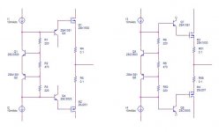
In looking at the loop gain of some idealized circuits in this configuration (just ideal controlled sources and no EF in the loop) I convinced myself that the Miller loop gain of this configuration, in the region where it is flat with frequency, is exactly its current gain. Maybe this is obvious to you, but it was not to me. Anyway, having a current gain of around 6.8x was the source of the Miller loop instability. The Miller loop gain magnitude wanted to stay flat, or even peak a little, in the region of tens of MHz where its phase was dropping off a cliff. In desperation, I tried the series RC networks shown below in the current mirror to reduce the current gain to about 1 at high frequencies. I thought this might ruin the distortion and the slew rate at the expense of stability. Not so. I was able to get a 90 degree phase margin in the Miller loop, without degrading either the slew rate or the distortion at all. So I'm a happy camper now. I may try more exotic compensation techniques later, but it's not obvious to me how to stabilize the Miller loop for these. I'll have to think about that some more.
As it stands now, bias current in the drivers are 30 mA, 15 mA in the predriver, 10 mA in the "VAS" and about 1.85 mA in the input stage.
Edmond Stuart said:One more thing: I feel uncomfortable with the high power dissipation in Q7 and Q8. Why not using simple 1:1 current mirrors and adding an extra class AB EF stage before the drivers?
I had looked at this briefly in the past and had oscillations. I was also having other problems at the time, so I didn't pursue it further back then. Since things were more stable now (or so I thought), I decided to revisit the predriver idea.
I did indeed see oscillations again when the predriver was added, and tracked it down to a local Miller loop instability. I was initially able to get it barely stable by putting base resistors in the CB stage of the Hawksford cascode, and based on this data, I found that under high-slew conditions, the total peak base currents into the predriver were about half of those into the driver. Not as much of an improvement as I would have hoped, but it gave hope for reducing the "VAS" current from 30 mA to 10 mA, which would then allow replacing the 2SC4793/2SA1837 cascode transistors with KSA1381/KSC3503. I also got a slight reduction in distortion, presumably due to lighter loading on the "VAS".
This led to the need for analyzing the local Miller loop gain. With non-complementary circuits, I have always done this by blocking the global feedback (for all but DC) by putting a huge series inductor and shunt capacitor in the global feedback loop, then putting a loop gain probe inside the Miller loop. This results in a bandpass filter-like response for the Miller loop gain exactly as expected. But when I try this with complementary circuits, the results are nonsense. I had almost given up on this, but then I realized that for this configuration at least, it's possible to artificially join the two halves at the Miller feedback pickoff point and put the loop gain probe there. See the picture below. The simulated Miller loop gain of this configuration is just as I expected.
In looking at the loop gain of some idealized circuits in this configuration (just ideal controlled sources and no EF in the loop) I convinced myself that the Miller loop gain of this configuration, in the region where it is flat with frequency, is exactly its current gain. Maybe this is obvious to you, but it was not to me
. Anyway, having a current gain of around 6.8x was the source of the Miller loop instability. The Miller loop gain magnitude wanted to stay flat, or even peak a little, in the region of tens of MHz where its phase was dropping off a cliff. In desperation, I tried the series RC networks shown below in the current mirror to reduce the current gain to about 1 at high frequencies. I thought this might ruin the distortion and the slew rate at the expense of stability. Not so. I was able to get a 90 degree phase margin in the Miller loop, without degrading either the slew rate or the distortion at all. So I'm a happy camper now. I may try more exotic compensation techniques later, but it's not obvious to me how to stabilize the Miller loop for these. I'll have to think about that some more.As it stands now, bias current in the drivers are 30 mA, 15 mA in the predriver, 10 mA in the "VAS" and about 1.85 mA in the input stage.
Attachments
Oh, and back to YAP itself...
We were talking about the possibility of adding a diamond buffer EF to the input of YAP, and also the concern about the high current in the feedback resistor in the fault condition. I was thinking that if the protection circuit turned off the current sources of this input diamond buffer, that would eliminate the high fault current (by depriving the input EFs of base current) and maybe also eliminate the need to separately shut down the "VAS" as well. Does this make sense or am I all wet?
We were talking about the possibility of adding a diamond buffer EF to the input of YAP, and also the concern about the high current in the feedback resistor in the fault condition. I was thinking that if the protection circuit turned off the current sources of this input diamond buffer, that would eliminate the high fault current (by depriving the input EFs of base current) and maybe also eliminate the need to separately shut down the "VAS" as well. Does this make sense or am I all wet?
andy_c said:Hi Ovidiu,
Earlier in this thread there was some discussion of diamond buffer vs. conventional EF drivers for the MOSFET OPS. You mentioned you saw higher crossover distortion with the conventional drivers. I was thinking about this earlier, and it dawned on me that for the Toshiba MOSFETS with conventional drivers, the bias spreader voltage will be about 4.4V (2 * 1.6 + 2 * 0.6), assuming 1.6V for each MOSFET and 0.6V for each BJT driver. For the diamond buffer, this voltage will be about 2.0V (2 * 1.6 - 2 * 0.6).
Since the tempco of the bias spreader is proportional to its voltage, this says the bias spreader tempco for the conventional driver case will be about 2.2x the tempco for the diamond buffer case. Could it be that the MOSFET bias for the conventional buffer case was overcompensated for temperature?
Andy,
I've concluded there's not much of a connection between the temperature overcompensation in the EF buffer and the cross conduction performance in YAP.
If you are looking at the attached bias spreader (left, as used in YAP), the Vbe multiplying factor is 2*(R1+R2+R3)/R2. The same multiplying factor obviously applies to the spreader tempco.
On the other side, the MOSFETs tempco multiplying factor is 2*(1+R4*gm). Note that the R4*gm represents, for a typical class AB implementation, a contribution of not more than 5-10% (totally different for a class A output stage).
My 2SK1530/2SJ201 pairs need about 1.8V (each) for a drain current of 150mA. Substract one Vbe of 0.6V for the diamond buffer Q3 and this leads to a Vbe multiplying factor of 2 per output device, resulting in a total spreader tempco of about 2.2*2*2=9.2mV/C.
Now, the diamond buffer dissipates around 0.5W and uses a 60C/W onboard heatsink. Which means the diamond buffer runs at about 55-60 degrees centigrades and hence one can barely consider the diamond buffer Vbe as a constant.
In practice, on the two output stage boards that I have built and measured, the bias starts at 200mA/device (at 25 degrees centigrades) and reaches 160mA after 1 hour at full power (200W into 4ohm) when the heatsink temperature is around 85-90 degrees centigrades. This makes for the drain current a variation of 0.66mA/C (which I think it's pretty good). Roughly, this is equivalent to a Vgs tempco overcompensation of about 1mV/C per device or 2mV/C between the spreader and the output devices (this is because the Id variation vith temperature is the Vgs variation with temperature multiplied by the device transconductance; 2SK1530 has a transconductance of about 0.7S at Id=150mA). One could of course to increase the output devices tempco by increasing R4/R5 - and get a better match, although this method would come to a price.
For simplicity, assume the diamond buffer and the output devices at the same temperature, this would mean that the diamond buffer effectively lowers the output stage tempco by 2.2mV/C per leg or 4.4mV/C per total. Given the spreader calculations above, this would render an output stage tempco of 13.4mV/C, or 6.7mV/C per device. Now, taking into account the experimental overcompensation above of 1mV/C per device, this leads to a 6.7-1=5.7mV/C tempco of each MOSFET output device. I have measured some time ago the 2SK1530 tempco, and I was quite suprised to find a pretty low average (of about 6mV/C) and a large dispersion (5-7mV/C). Anyway, this independently measured average value of 6mV/C matches pretty well the YAP measured/calculated value of 5.7mV/C. The slight difference could be due to the assumption the diamond buffer and the output devices are at same temperature.
Now, in the other case, of a regular buffer, and using the above data, the spreader multiplying factor has to be 3 per output device, leading to a total spreader tempco of 13.2mV/C.
Following the same pattern as above (the EF buffer would have about the same dissipation) and considering 5.7mV/C for the output devices, this will lead to a tempco mismatch (per device) of 5.7+2.2-13.2/2=1.3mV/C, which would lead under the same condition to a bias Id variation of 0.9mA/C or 54mA for 25-85 degrees centigrades variation. Compare this to the 40mA variation for the diamond buffer.
Therefore, while certainly the diamond buffer helps in minimizing the MOSFETs to Vbe multiplier tempco mismatch, I would not say there should be a significant difference in terms of cross conduction...
Attachments
Miller
Hi Andy,
Now things are getting interesting, as I encountered the same problems with the Miller compensation and I'm using the same technique (an additional lead-lag network) to suppress oscillations of the VAS.
Before going further I like to know some details:
The value of Cci, Rci, Cx and ULG of the Miller loop.
Also, what kind of output stage, BJTs or MOSFETs and how many of them?
How high are your 'high-slew conditions' (in V/us)?
I'm asking this because I'm amazed why you need so much VAS bias current.
BTW, the VAS of my (still virtual) amp draws only 4.5mA and at 100kHz sine and full power, the AC component is less than 1mA-pk-pk. (OPS: 4 pair of MOSFETs + driver, no pre-driver, VAS current gain=24dB ).
Regards,
Edmond.
andy_c said:[snip]
In desperation, I tried the series RC networks shown below in the current mirror to reduce the current gain to about 1 at high frequencies. I thought this might ruin the distortion and the slew rate at the expense of stability. Not so. I was able to get a 90 degree phase margin in the Miller loop, without degrading either the slew rate or the distortion at all. So I'm a happy camper now. I may try more exotic compensation techniques later, but it's not obvious to me how to stabilize the Miller loop for these. I'll have to think about that some more.
As it stands now, bias current in the drivers are 30 mA, 15 mA in the predriver, 10 mA in the "VAS" and about 1.85 mA in the input stage.
Hi Andy,
Now things are getting interesting, as I encountered the same problems with the Miller compensation and I'm using the same technique (an additional lead-lag network) to suppress oscillations of the VAS.
Before going further I like to know some details:
The value of Cci, Rci, Cx and ULG of the Miller loop.
Also, what kind of output stage, BJTs or MOSFETs and how many of them?
How high are your 'high-slew conditions' (in V/us)?
I'm asking this because I'm amazed why you need so much VAS bias current.
BTW, the VAS of my (still virtual) amp draws only 4.5mA and at 100kHz sine and full power, the AC component is less than 1mA-pk-pk. (OPS: 4 pair of MOSFETs + driver, no pre-driver, VAS current gain=24dB ).
Regards,
Edmond.
syn08 said:I've concluded there's not much of a connection between the temperature overcompensation in the EF buffer and the cross conduction performance in YAP.
Hi Ovidiu,
That's quite an analysis there! The whole temperature compensation thing is really a can of worms, isn't it?
I ended up just giving up on trying to analyze or simulate it. With the IRF/Fairchild devices, the bias spreader voltage ends up being quite large, so what I'll do is put a normal Vbe multiplier in series with a TL431 or similar. I'll put pots in both of these, in effect making a bias spreader with adjustable tempco. Once I figure out the optimum tempco, I'll just replace the pot in the Vbe multiplier with a fixed resistor and use the pot in the TL431 to adjust bias.
andy_c said:
Hi Ovidiu,
That's quite an analysis there! The whole temperature compensation thing is really a can of worms, isn't it?
I ended up just giving up on trying to analyze or simulate it. With the IRF/Fairchild devices, the bias spreader voltage ends up being quite large, so what I'll do is put a normal Vbe multiplier in series with a TL431 or similar. I'll put pots in both of these, in effect making a bias spreader with adjustable tempco. Once I figure out the optimum tempco, I'll just replace the pot in the Vbe multiplier with a fixed resistor and use the pot in the TL431 to adjust bias.
One problem with TL431 is stability. I had some really nasty suprises with this critter, including a large PCB redo ($$$).
Look at the datasheet http://focus.ti.com/lit/ds/symlink/tl431.pdf fig.16 and note the stability in capacitive loads. For whatever reason, Fairchild doesn't even mention such issues and goes so far in showing TL431 directly decoupled with a cap (which is definitely a no-no)! Now, I'm not saying it's going unstable for whatever cap load, but certainly the risk is there and it can get really ugly. I've tried to simulate this kind of stability issue and I got (with the default/stock models), of course, nothing.
andy_c said:
Hi Ovidiu,
That's quite an analysis there! The whole temperature compensation thing is really a can of worms, isn't it?
I ended up just giving up on trying to analyze or simulate it. With the IRF/Fairchild devices, the bias spreader voltage ends up being quite large, so what I'll do is put a normal Vbe multiplier in series with a TL431 or similar. I'll put pots in both of these, in effect making a bias spreader with adjustable tempco. Once I figure out the optimum tempco, I'll just replace the pot in the Vbe multiplier with a fixed resistor and use the pot in the TL431 to adjust bias.
Yes, it can be a can of worms!
One problem with TL431 is stability. I had some really nasty suprises with this critter, including a large PCB redo ($$$).
Look at the datasheet http://focus.ti.com/lit/ds/symlink/tl431.pdf fig.16 and note the stability in capacitive loads. For whatever reason, Fairchild doesn't even mention such issues and goes so far in showing TL431 directly decoupled with a cap (which is definitely a no-no)! Now, I'm not saying it's going unstable for whatever cap load, but certainly the risk is there and it can get really ugly. I've tried to simulate this kind of stability issue and I got (with the default/stock models), of course, nothing.
Re: Miller
Hi Edmond,
ULG of the Miller loop is about 20.5 MHz. At 1 MHz, the Miller loop gain is 1.1 dB down from its max value of 15.2 dB at 27 kHz. Cx is 100 pF. Cci is also 100 pF. Rci is zero. I know the latter sounds strange for a CFB stage, but when the feedback is taken from the VAS collector, I've observed that the best Miller loop stability occurs when Rci is zero. Based on only a very quick and preliminary look, just the opposite seems to be true when the feedback is taken from the predriver emitter - Rci needs to be non-zero in that case.
10+10 IRFP244/FQA9P25. Simulation uses EKV models I've developed for these.
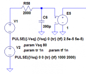
I'm trying to get non-slewing behavior with a square wave input of +/-80V, low-pass filtered by a buffered 2k/390pF filter. See the attachment below. This gives about 205 V/us. I vary R58 to adjust the max dv/dt of this signal as needed.
I see I've caused some confusion, mostly because I'm confused myself! Here's what happened. In early simulations with this square wave signal, I found that the output would completely go crazy when one of the VAS transistors would cut off. I did a bandaid of increasing the VAS current for this reason. But this was before I figured out how to get meaningful Miller loop gain sims by joining the complementary halves of the circuit as in my post #270 above. Once I was able to do so, I realized that my prior experiments were with a VAS that, while not an oscillator, was only marginally stable. I believe there was some kind of large-signal instability triggered by one of the VAS transistors going into cutoff. Once I was able to get a robust phase margin in the Miller loop using the series RC compensation network, I found there was no problem at all when cutoff occurs under high-slew conditions. In this case, the input stage cuts off and the VAS does not. I'd like to go back and experiment with reducing the VAS current still more (it's 10 mA now), and also eliminating the predriver. I haven't done this yet though.
Yes, as far as sine waves go, peak currents are very low. What I'm doing is applying a stimulus to the circuit as shown in the attachment below (or to parts of the circuit like the driver/OPS combo by itself). I look at the peak current through E5. This can be unexpectedly high. For example, with a diamond buffer input at the front end of the output stage, the peak value of the sum of the base currents is in the uA range with an 80 Volt peak sine wave at 20 kHz. Yet when the 80 Volt peak square wave below is applied, I get about +/- 15 mA. (BTW, the odd arrangement of two series sources is to get a square wave that starts at zero Volts, then goes to +/- 80 Volts thereafter).
Hi Edmond,
Edmond Stuart said:Before going further I like to know some details:
The value of Cci, Rci, Cx and ULG of the Miller loop.
ULG of the Miller loop is about 20.5 MHz. At 1 MHz, the Miller loop gain is 1.1 dB down from its max value of 15.2 dB at 27 kHz. Cx is 100 pF. Cci is also 100 pF. Rci is zero. I know the latter sounds strange for a CFB stage, but when the feedback is taken from the VAS collector, I've observed that the best Miller loop stability occurs when Rci is zero. Based on only a very quick and preliminary look, just the opposite seems to be true when the feedback is taken from the predriver emitter - Rci needs to be non-zero in that case.
Also, what kind of output stage, BJTs or MOSFETs and how many of them?
10+10 IRFP244/FQA9P25. Simulation uses EKV models I've developed for these.
How high are your 'high-slew conditions' (in V/us)?
I'm asking this because I'm amazed why you need so much VAS bias current.
I'm trying to get non-slewing behavior with a square wave input of +/-80V, low-pass filtered by a buffered 2k/390pF filter. See the attachment below. This gives about 205 V/us. I vary R58 to adjust the max dv/dt of this signal as needed.
I see I've caused some confusion, mostly because I'm confused myself! Here's what happened. In early simulations with this square wave signal, I found that the output would completely go crazy when one of the VAS transistors would cut off. I did a bandaid of increasing the VAS current for this reason. But this was before I figured out how to get meaningful Miller loop gain sims by joining the complementary halves of the circuit as in my post #270 above. Once I was able to do so, I realized that my prior experiments were with a VAS that, while not an oscillator, was only marginally stable. I believe there was some kind of large-signal instability triggered by one of the VAS transistors going into cutoff. Once I was able to get a robust phase margin in the Miller loop using the series RC compensation network, I found there was no problem at all when cutoff occurs under high-slew conditions. In this case, the input stage cuts off and the VAS does not. I'd like to go back and experiment with reducing the VAS current still more (it's 10 mA now), and also eliminating the predriver. I haven't done this yet though.
BTW, the VAS of my (still virtual) amp draws only 4.5mA and at 100kHz sine and full power, the AC component is less than 1mA-pk-pk. (OPS: 4 pair of MOSFETs + driver, no pre-driver, VAS current gain=24dB ).
Yes, as far as sine waves go, peak currents are very low. What I'm doing is applying a stimulus to the circuit as shown in the attachment below (or to parts of the circuit like the driver/OPS combo by itself). I look at the peak current through E5. This can be unexpectedly high. For example, with a diamond buffer input at the front end of the output stage, the peak value of the sum of the base currents is in the uA range with an 80 Volt peak sine wave at 20 kHz. Yet when the 80 Volt peak square wave below is applied, I get about +/- 15 mA. (BTW, the odd arrangement of two series sources is to get a square wave that starts at zero Volts, then goes to +/- 80 Volts thereafter).
Attachments
syn08 said:One problem with TL431 is stability. I had some really nasty suprises with this critter, including a large PCB redo ($$$).
I hear you! I've been using the behavioral model by analogspiceman from the LTspice user's group. It simulates the frequency dependence of the loop gain, and I've been able to do loop gain sims and see this unstable behavior with capacitive loads. I will definitely look into it further though.
How about the LM385? Have these been stable for you? I noticed you're using 0.1 uF in parallel with these. Have you tried the LM336?
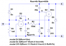
* TL431A behavioral model by analogspiceman
.SUBCKT TL431_A A K R
R1 R A 1e6
D4 A 4 2V5
D5 A K Dc
D1 R K Dc
G2 K 4 6 A 90m
G1 A 5 R 4 1
C1 5 A 1n Rpar=1k
R2 6 5 700k
D2 4 R Dc
D3 A 6 Di
C2 K 6 40p Rser=6k Rpar=400k
.model Di D(Ron=10m)
.model Dc D(Ron=7 Vfwd=.6 Vrev=36)
.model 2V5 D(Ron=.13 Vfwd=.6 Vrev=2.5 Roff=7k)
.ENDS
Attachments
andy_c said:
How about the LM385? Have these been stable for you? I noticed you're using 0.1 uF in parallel with these. Have you tried the LM336?
LM385 is my favorite for a low voltage reference. It's stable, never had issues with. Haven't tried the LM336.
I'll take a look at the model.
I received over the holidays several emails complaining about www.synaesthesia.ca being down.
There's nothing wrong with the site by itself. The site statistics shows about 1,500-2000 visits every month (consistent with the site counter that monitors new visitors only) with about 5Gb/month download traffic. The provider (INTERNIC Canada) is up, healthy, well connected to the Internet core and has also all peering connections working fine.
Any difficulties are most likely because of local ISP issues. A tracert to www.synaesthesia.ca will show where the connection gets stuck. If tracert fails without any progress, then it is most likely a DNS problem. There are several ways to diagnose this, but essentially if after a ipconfig /flushdns (on windows) the problem persists, then please contact your ISP. They may have an outdated DNS cache or a problem with the dynamic routes update.
- Status
- This old topic is closed. If you want to reopen this topic, contact a moderator using the "Report Post" button.
- Home
- Amplifiers
- Solid State
- YAP - Yet Another PowerAmp