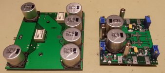
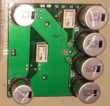
Here is the finished regulator...
+-15V
+-15V
An externally hosted image should be here but it was not working when we last tested it.
Hi Coris...
Im just about finished building my regulator/PSU...just waiting on transformer.
I plan on inserting power from the back of the STX into the filtering caps (not sure if Im going to remove them or not yet). V+ and V- both have a ground on the STX...my regulator shares the same ground for both + and -. Do I want to run 2 ground wires to the STX from the regulator, each twisted with their own V wire to reject EMI...?
Or a single ground, and bridge the two ground pins on the filtering caps?
It looks like in the pic, you scraped away some of the silk screening at the cap positions to get more solderable area...?
Hi Wungun
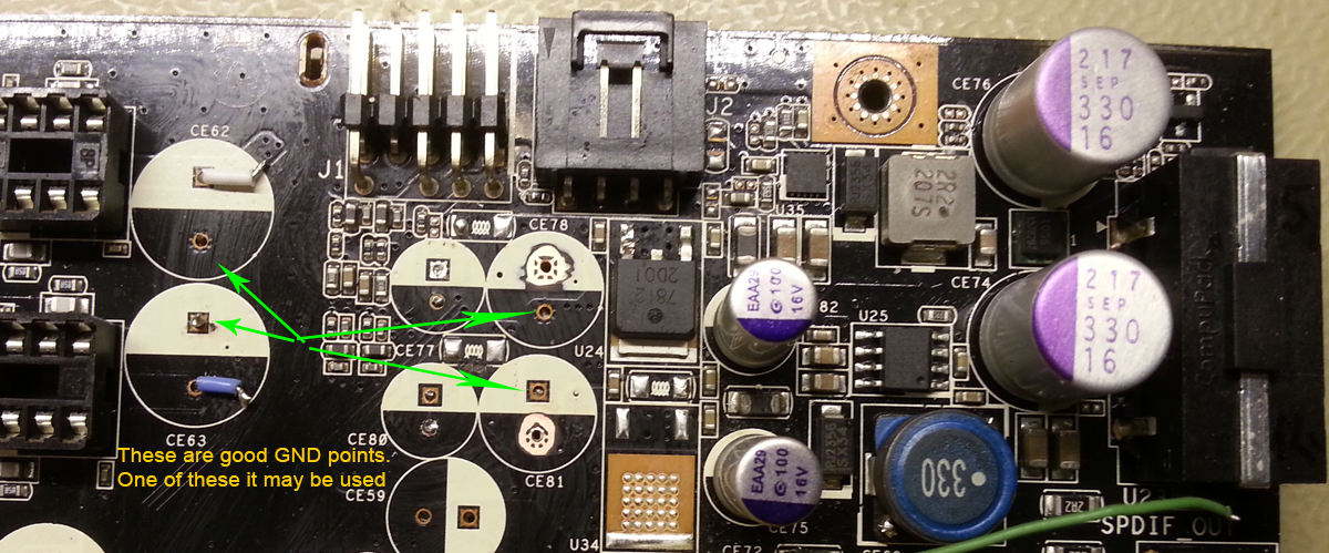
There is all right with one GND connection from your PSU to the board, if your PSU it have common ground. Ideally the power regulator`s GND should not be common on the PSU board, but meet together on the sound card. But is OK in your case. The connection it may be just short as possible, and it should be better to have few wires for this connection... I mean few reasonable thin wires (soldered in the same GND point) is better than only one thick wire.
You can see in my previous pictures a good place for GND connection on the sound card.
I think Ill remove those 2 filtering caps and solder there, on the top of the card....
Trying to follow what you mean...I have seprate grounds from trans to the input of the regulator, and a common ground out...
Should the single ground from my regulator out "split" to be soldered to the 2 negative poles of the two caps...bridged? I think you mean its better to run 2 ground wires...? I dont see in your pics where you have your ground. I assume its to both capacitors, CE78 and CE81? I think both grounds on the STX are common/series mounted caps, so connecting to one point is okay...
Thansk for your feedback! Should have this running this week!
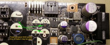
Hello Coris I took the module from Texas Instruments as recommended by you, I can remove the capacitors C77-C78-C80-C81 and C59 analog CE62 and CE63 connect V + and V-and GND directly on CE62 and CE63 as your photo http://www.diyaudio.com/forums/atta...4d1395615196-xonar-st-stx-mods-gnd-points.jpg ?
Can I solder directly to the back of the card without passing the plate?
Thank you.
Can I solder directly to the back of the card without passing the plate?
Thank you.
Last edited:
Hi ciccio1112
There is not so necessary to remove these caps if you plan to use another bigger one in parallel. More important is to remove the right components to isolate the computer/board power system from the one you will add. None that the caps in case are quite difficult to be desoldered, without good tools, and skills.
Of course you can solder the wires on the back of the card, where is indicated on picture. Please pay attention to the C62/63. There is in the picture two small pins (blue and white) which represent the connection points for -V and +V respectively (white - V+). The common ground of the caps is a good GND connection for the new PSU.
Coris, I removed caps on another Xonar board by breaking their legs. I tried removing them by desoldering, it was hard. I was afraid I could destroy the board so I stopped. Do you have any tip on desoldering them. I used a lot of desoldering iron and 305C temperature (which I use 99% time). No effect.
Hi Corvus5
Welcome back...")
Yes is hard to desolder the caps out of the board. Breaking their legs is the best way to remove it. Strongly recommended!
The sound card`s PCB is very easy destroyable when touch it with a regular soldering iron. There is not here about only the temperature of the soldering iron, but it is too, about its heating power in the soldering point. This power it is function the dissipation of the heat into the copper to be soldered... There is a soldering station (induction) type which should be used when modding such sensitive PCBs. That it rigorously control/adjust both the heating power and the temperature at the soldering point, so that one never destroy the traces. But this is quite expensive...
Honestly, this kind of mod, when one it may replace the original caps with better ones, belong now to the "stone age"... The main point modding the Xonar is to give it a better PSU, and replacing its post DAC analogue stage... And a better clock... and some more details...
But do not worry, it will come (hope soon) the mod where is no longer necessary to remove something from the board. But only adding a small daughter boards system. New designed and fully isolated DAC & analogue, with its independent power system (lowest noise floor with the today ultimate technology), which it will use (connect it to) only the DAC digital interface (I2S) from the original sound card.
The PCBs have arrived. It still only to be populate it and test it... Maybe next week it will come out some pictures...
My prototype just sounds fantastic (better than I could get out of an ESS9018 DAC...), but the final design is even more improved. I`m very excited to put all together, to hear it, and see some measurements...
Welcome back...
Yes is hard to desolder the caps out of the board. Breaking their legs is the best way to remove it. Strongly recommended!
The sound card`s PCB is very easy destroyable when touch it with a regular soldering iron. There is not here about only the temperature of the soldering iron, but it is too, about its heating power in the soldering point. This power it is function the dissipation of the heat into the copper to be soldered... There is a soldering station (induction) type which should be used when modding such sensitive PCBs. That it rigorously control/adjust both the heating power and the temperature at the soldering point, so that one never destroy the traces. But this is quite expensive...
Honestly, this kind of mod, when one it may replace the original caps with better ones, belong now to the "stone age"... The main point modding the Xonar is to give it a better PSU, and replacing its post DAC analogue stage... And a better clock... and some more details...
But do not worry, it will come (hope soon) the mod where is no longer necessary to remove something from the board. But only adding a small daughter boards system. New designed and fully isolated DAC & analogue, with its independent power system (lowest noise floor with the today ultimate technology), which it will use (connect it to) only the DAC digital interface (I2S) from the original sound card.
The PCBs have arrived. It still only to be populate it and test it... Maybe next week it will come out some pictures...
My prototype just sounds fantastic (better than I could get out of an ESS9018 DAC...), but the final design is even more improved. I`m very excited to put all together, to hear it, and see some measurements...
Last edited:
There's no reason to stay with the card when you can build your own or use different board. This is the card for fast and easy improve in sound. On my own USB interface/DAC/amp I use a lot of eneloops, high quality caps (had to buy some directly in Akihabara) and very high quality resistors, special cables, custom made headphone drivers. Totally different, once it was fantastic but there's still place for improvements. On the Xonar however a lot of things are set. Injecting I2S and own power and amp leaves only DAC chip and CMI chip on board. Is it worth?
I think is worth. At least my developed system it can be attached to any I2S interface, or the post DAC processing and its own power system it can be used as a stand alone module on every kind of DAC system. The advantage of ST/STX is the already existent driver, a good integration with the PC/OS system, the capability of digital record/playback 192khz/24bit/32bit, and even 64bit. The only weak part of this sound card is its analogue stage and its related power, and the clock oscillators...
Massacring up an original board, adding caps and destroy the PCB traces, desolder and solder back components, and a chaos of the signal paths on a modified sound card it can not be at all a real improvement. Putting all together in a professional meaner is anyway a better way to go. My system is very easy to be implemented/added in place.
Massacring up an original board, adding caps and destroy the PCB traces, desolder and solder back components, and a chaos of the signal paths on a modified sound card it can not be at all a real improvement. Putting all together in a professional meaner is anyway a better way to go. My system is very easy to be implemented/added in place.
Last edited:
I have some pictures of the battery powered clock(s) mod for STX/ST (or for what so ever application). Unfortunately this assembly is not in its final edition, because I discovered some design faults. But the pictures are good to give an idea about.
As the new PCBs will be in place, this mod it may be available for interested ones.
There is place for four (different sized) oscillators on the board, but any kind of oscillator it can be adapted to the existing footprints. Of course this assembly it can be used to clock what so ever. One may only solder the right oscillators in place. The connections between board (oscillators output) it will be made by coax (which it will come together in the kit). The battery is powerful enough to furnish power to the clocks for more than 24 continuous hours. When the device is off, the battery is charged (monitored by specialized chip on board). The charger GND and the device GND are not common on the board. Once the device is on, the board disconnect completely the charger`s GND/Vcc.
Attachments
Great coris I would be interested is ALREADY AVAILABLE daughter card has a cost?
You spoke well of I2S interface you have some more info?
Thank you.
See you soon.
In fact this (battery) PCB it have a design fail (that because is not pictured the backside... But is usable actually, as this one assembled.
The right PCB is in production now...
Yes, the PCBs of the DAC with I2S interface is ready (waiting) to be populated/assembled. Actually I have ready all the PCBs for the whole system, and to populate these it will be my first priority for the next weeks.
Last edited:
Is it a lithium ion battery?
The copper pour on the top also could do with some stitching vias down to the GND pour on the bottom, I presume there is one?
Yes, there is a 2,3Ah mobile phone battery.
Your presumption is right. But the backside GND plane is not connected with the upper one, and is used as heat sink for the charger system (different GND...).
When the right PCB will be ready, you may see the picture of the backside too...
The assembling is going on...
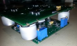
The PSU is already finished. I`m working now on the post DAC processing module, which is partially assembled too.
There are here some pictures, to give you an idea about the system...
The PSU is already finished. I`m working now on the post DAC processing module, which is partially assembled too.
There are here some pictures, to give you an idea about the system...
Attachments
Last edited:
- Home
- Source & Line
- PC Based
- Xonar ST/STX mods...