Hi all!
I'm on finishing stages of crossover PCB development, and need yours input on my design.
The crossover board consists of:
- Input LPF for HF noise elimination (passive stage)
- Gain/input buffer with limited bandwidth feedback
- Bafflestep
- Single global notch + buffer after the notch
- LP for woofer
- HP for midrange
- Variable phase for midrange
- LP for midrange
- HP for tweeter
- Variable phase for tweeter
- Each output stage for woofer,mid,tweeter consists of single notch + output buffer.
The filters chaining is as described at LinkwitzLab.com - the tweeter signal travels the following path:
- Input - bafflestep - notch - hp mid - phase mid - hp tweeter - notch tweeter - output buffer, so there is no phase errors between woofers, midranges and tweeters.
Currently i'm doing the following tasks:
- Upgrading the PSU - from simple chunked-up capacitors to LM317/337 regulators on board (they shouldn't produce much heat)
- Adding optional balanced input at input stage (simple single opamp scheme)
- Adding ability to bypass/reroute all the sections (say, you want to use it for full range speakers, but with 3 notches and no phase shifter? no problem!, just chain-up the output notches and bypass the phase shifter/LP section).
- All the HP/LP filters are 2/4-th order (selectable), Sallen-Key topology.
- All the passive elements footprints allow placing both SMT and thru-hole components
- All the filtering capacitors could be up to ~40mm length, 5mm wide
- All the filter resistors are built from 4 paralleled/chained SMTs, or 2 paralleled thru-holes - for getting exact values from limited E12/E24 values range. (the values finder will be supplied as a windows program or web service - you type the required value, select E12/E24, and get the closest value from chained/paralleled resistors).
As a side note:
Each opamp bypassing circuit requires:
- 1206 NP0 ceramic caps (value range is around 1n-3n, or anything you have around, that is not too small for the application)
- 5mm diameter electrolytic cap (anything you have, rated at 16v+, 1uf+).
- Opamp sockets are required - you have to use the gold=plated ones with round pins - they stand out of PCB for a 1-2mm - this space is required for placing PSU bypassing SMT caps.
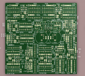
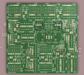
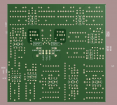
And... everything is stuck on 4x4in PCB! You'll need 2 boards for stereo.
Design highlights:
- Two-sided ground plane pours
- "Starry" power delivery to ICs
- Both SMTs and thru-hole components are possible in most cases, in various sizes (good for huge film caps)
Pricing guestimation? 10$-20$ for single board.
Ordering? You'll be able to buy the boards from seeedstudio.com, after i test/fix the first PCB batch for design errors.
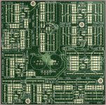
Attached are:
- Top/bottom board views without ground pours (to show the traces on opposite layers).
- Schematics in PDF (please disregard the component values, they are for layout purposes only).
Limitations... - board size, should be 4x4in - hence the tight layout.
I'm on finishing stages of crossover PCB development, and need yours input on my design.
The crossover board consists of:
- Input LPF for HF noise elimination (passive stage)
- Gain/input buffer with limited bandwidth feedback
- Bafflestep
- Single global notch + buffer after the notch
- LP for woofer
- HP for midrange
- Variable phase for midrange
- LP for midrange
- HP for tweeter
- Variable phase for tweeter
- Each output stage for woofer,mid,tweeter consists of single notch + output buffer.
The filters chaining is as described at LinkwitzLab.com - the tweeter signal travels the following path:
- Input - bafflestep - notch - hp mid - phase mid - hp tweeter - notch tweeter - output buffer, so there is no phase errors between woofers, midranges and tweeters.
Currently i'm doing the following tasks:
- Upgrading the PSU - from simple chunked-up capacitors to LM317/337 regulators on board (they shouldn't produce much heat)
- Adding optional balanced input at input stage (simple single opamp scheme)
- Adding ability to bypass/reroute all the sections (say, you want to use it for full range speakers, but with 3 notches and no phase shifter? no problem!, just chain-up the output notches and bypass the phase shifter/LP section).
- All the HP/LP filters are 2/4-th order (selectable), Sallen-Key topology.
- All the passive elements footprints allow placing both SMT and thru-hole components
- All the filtering capacitors could be up to ~40mm length, 5mm wide
- All the filter resistors are built from 4 paralleled/chained SMTs, or 2 paralleled thru-holes - for getting exact values from limited E12/E24 values range. (the values finder will be supplied as a windows program or web service - you type the required value, select E12/E24, and get the closest value from chained/paralleled resistors).
As a side note:
Each opamp bypassing circuit requires:
- 1206 NP0 ceramic caps (value range is around 1n-3n, or anything you have around, that is not too small for the application)
- 5mm diameter electrolytic cap (anything you have, rated at 16v+, 1uf+).
- Opamp sockets are required - you have to use the gold=plated ones with round pins - they stand out of PCB for a 1-2mm - this space is required for placing PSU bypassing SMT caps.
And... everything is stuck on 4x4in PCB! You'll need 2 boards for stereo.
Design highlights:
- Two-sided ground plane pours
- "Starry" power delivery to ICs
- Both SMTs and thru-hole components are possible in most cases, in various sizes (good for huge film caps)
Pricing guestimation? 10$-20$ for single board.
Ordering? You'll be able to buy the boards from seeedstudio.com, after i test/fix the first PCB batch for design errors.
Attached are:
- Top/bottom board views without ground pours (to show the traces on opposite layers).
- Schematics in PDF (please disregard the component values, they are for layout purposes only).
Limitations... - board size, should be 4x4in - hence the tight layout.
Attachments
Last edited:
Parametric EQ both subtracting and adding is a nice feature, will be added.
Rerouting the default signal path will be added too, yet i doubt it will be useful, as there are already enough features on each signal thread, and the topology is ok (as Linkwitz described on his site).
I'm playing right now with software, that going to simulate the crossover behavior (plotting graphs based on RC values in the circuit, and generating RC values based on sliders position). Going to be coded in VB.NET, and will require .NET framework, 3.0-3.5.
Say, you want to place a notch at some frequency. You move the F, then choose Q and depth, click "simulate" and get a picture how it will look like on frequency response.
A further step - is to load frequency response of each speaker in their enclosure, and tweak it visually by sliders, and then to get values for the implementation circuit.
Summing the response is a bit tricky, as there are phase/directivity issues of driver placement/size, so the flat frequency response won't tell the whole picture.
Maybe i'll do the "ideal" summed response, assuming every speaker get perfectly aligned phase, and then to get that response, user will need to tweak phase shifters to align phases in the real world.
The last, and furthermost option would be creation of software EQ/channel splitter, that will be able to play simulated filers using computer multichannel sound card. That's voodoo for me at this step of my evolution")
I'm okay on hardware DSPs, FIR/IIRs, yet i have no idea how to implement it on regular CPUs with regular C/C++. Probably some audio buffer processing.
Then, designing a speaker will be an easy task - throw in some amplifiers, build enclosures, play with filers in software, build them in hardware - and forget about filters existence as your darkest nightmare.
Rerouting the default signal path will be added too, yet i doubt it will be useful, as there are already enough features on each signal thread, and the topology is ok (as Linkwitz described on his site).
I'm playing right now with software, that going to simulate the crossover behavior (plotting graphs based on RC values in the circuit, and generating RC values based on sliders position). Going to be coded in VB.NET, and will require .NET framework, 3.0-3.5.
Say, you want to place a notch at some frequency. You move the F, then choose Q and depth, click "simulate" and get a picture how it will look like on frequency response.
A further step - is to load frequency response of each speaker in their enclosure, and tweak it visually by sliders, and then to get values for the implementation circuit.
Summing the response is a bit tricky, as there are phase/directivity issues of driver placement/size, so the flat frequency response won't tell the whole picture.
Maybe i'll do the "ideal" summed response, assuming every speaker get perfectly aligned phase, and then to get that response, user will need to tweak phase shifters to align phases in the real world.
The last, and furthermost option would be creation of software EQ/channel splitter, that will be able to play simulated filers using computer multichannel sound card. That's voodoo for me at this step of my evolution
I'm okay on hardware DSPs, FIR/IIRs, yet i have no idea how to implement it on regular CPUs with regular C/C++. Probably some audio buffer processing.
Then, designing a speaker will be an easy task - throw in some amplifiers, build enclosures, play with filers in software, build them in hardware - and forget about filters existence as your darkest nightmare.
Ok, as promised: The software tool for crossover simulation.
Just a screenshot...
What was done:
- Calculated transfer functions for HP, LP, Bafflestep, Notch for the circuits i have. Each trandfer functions receives a R,C,f parameters as input and returns a magnitude for particular combination of resistors, caps and frequency, in complex way.
- Made some kind of "platform" for transfer function analysis - graphing, frequency sweep, layered display of graphs.
To do:
- Calculate a phase transfer function.
- Add some controls! Changing Q, F, depth e.t.c for filters > calculation of actual R,C values > Simulation.
- Chaining functions. Probably by complex multiplication, and then plotting as it was single function.
- Frequency response loading. That will be a hard thing to do. I'd like to split it into 2 steps:
- - Graphical graph loading and analysis - datasheet graphs could be used, as well as any other.
- - Data import from major measurement programs (LEAP, ARTA, LspCAD etc).
- Phase, phase phase. I have to think what to do with it... Importing the phase graphs of measured speakers should be nice, and alteration of the graph based on phase filter response - even better.
Attachments
I wonder whether it's sufficient to put just a single first order all-pass circuit on tweeter output? Won't i almost always need at least two all-pass stages?
In the other hand, the woofer-midrange physical offset shouldn't affect the frequency response, as the phase difference between woofer-midrange acoustical centers are really small...
So it's better to use both all-pass networks just on tweeter's filter...?
In the other hand, the woofer-midrange physical offset shouldn't affect the frequency response, as the phase difference between woofer-midrange acoustical centers are really small...
So it's better to use both all-pass networks just on tweeter's filter...?
UAF42 board for 2nd order filter, equalizer, active crossover
I have finally arrived at a scheme using the UAF42 IC from Burr Brown for line level crossovers in active speakers. Each UAF42 IC has simultaneous outputs for second order LP, BP, and HP functions. What is very nice is that, using three multi-turn trim pots, I can independently adjust Q and crossover frequency of each section. One circuit can be used for any 2nd order filter function within the audio band, making it more or less "universal".
I recently realized a way to used the bandpass output to make a single band, variable Q, variable frequency, second order equalizer section. The Q and center frequency are varied using the UAF42s controls, and another circuit takes the BP output and turns it in to a boost or cut.
In addition to these functions, I have a separate board that will handle input (balanced or single ended), and baffle step with a variable center frequency and attenuation.
These are pretty much all the building blocks that you need to make active crossovers for speakers. The second order sections can be cascaded to make higher order filters and the equalizer can be used to notch out resonances, fill in dips in the frequency response, remove the hump in the baffle step response, etc.
I don't have custom PCBs for these, so I am using a general IC prototyping board that has some traces on it. Several of these boards are needed depending on how many filter stages and equalization bands are used. Since the prototyping boards are all the same size, I can easily mount them together inside a speaker somewhere as a stack.
If any one is interested in collaborating on a run of custom PCBs for this kind of thing, please contact me. I don't have any experience in PCB design, routing, etc. for low level signals so I am a little out of my league. That's why for now I am only using the pre-fab boards. But I think a lot of people would be interested in this kind of PCB because amplification that you can put in a speaker is cheap and plentiful. The one thing that is missing to allow people to easily build their own active speakers are the line-level crossover boards. Since I have figured out a way to make a universal crossover with the UAF42, which I can get on Ebay for under $2 US each, this would be a great way to get more people interested in to speaker building. If you are a company selling chip amps, wouldn't this be a great match to your product line???
-Charlie
Not at all wishing to rain on your parade, but a few things about the UAF42 on the surface don't bode too well for getting good sound. Firstly the THD is 0.1% and only specified at 1kHz and unity gain. There's the likelihood of more severe HF distortion than this and it'll also get worse at higher gains. The GBW product of the opamps looks barely adequate for audio at 4MHz. The quiescent current for 4 JFET input amps is a fairly measly 6mA - that's just 1.5mA per opamp. Finally, as the list price for these is over $7 (1k), how do you know the eBay parts aren't fakes?
that's not what I measured
Thanks for mentioning the specs from the datasheet. Honestly, I don't believe that that the bandwidth is a problem. You are not using the chip as a gain stage, it's a filter and the gain will be unity or less, so I think that there is plenty of GBP.
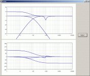
On the other hand, the THD spec would be worrisome, except that I have built and measured a circuit using this chip. The actual circuit construction was pretty ugly, I didn't do any bypassing, I took the measurements without any special attention to shielding, etc. and I still got way less distortion than 0.1%, in fact it is less than 0.01% at all frequencies and is generally below 0.005%. OK, I just noticed that I only measured 2nd and 3rd order distortion, and the measurements only go up to 500Hz (this was a low frequency HP filter), but you get the idea. See image below...
Here is a graph of the distortion of the circuit from my project using the UAF42:

-Charlie
Thanks for mentioning the specs from the datasheet. Honestly, I don't believe that that the bandwidth is a problem. You are not using the chip as a gain stage, it's a filter and the gain will be unity or less, so I think that there is plenty of GBP.
On the other hand, the THD spec would be worrisome, except that I have built and measured a circuit using this chip. The actual circuit construction was pretty ugly, I didn't do any bypassing, I took the measurements without any special attention to shielding, etc. and I still got way less distortion than 0.1%, in fact it is less than 0.01% at all frequencies and is generally below 0.005%. OK, I just noticed that I only measured 2nd and 3rd order distortion, and the measurements only go up to 500Hz (this was a low frequency HP filter), but you get the idea. See image below...
Here is a graph of the distortion of the circuit from my project using the UAF42:
-Charlie
Last edited:
Thanks for sharing the plot. It looks like you've a very low fundamental frequency there - with the harmonics below 100Hz, you might be looking at 10 - 30Hz for the fundamental. That's not inconsistent with the datasheet figure at 1kHz, here's why.
The opamps in your chip look to have very similar performance characteristics to the TL074 (with the exception of THD - on the TL074 its low, around 0.003% at 1kHz.) So its reasonable to assume the OL gain curve is going to look similar to the TL074. This part shows an OL -3dB bandwidth around 50Hz. There's a factor of 20 between this and 1kHz, so the distortion will be the same factor higher there. That's for me the explanation of the difference between 0.005% and 0.1%.
The opamps in your chip look to have very similar performance characteristics to the TL074 (with the exception of THD - on the TL074 its low, around 0.003% at 1kHz.) So its reasonable to assume the OL gain curve is going to look similar to the TL074. This part shows an OL -3dB bandwidth around 50Hz. There's a factor of 20 between this and 1kHz, so the distortion will be the same factor higher there. That's for me the explanation of the difference between 0.005% and 0.1%.
There is no fundamental, that might be power supply noise or something similar.
This measurement was done using swept sine or white noise input, can't recall which. This is the distortion spectrum, not the noise floor plus some harmonics of a single tone.
-Charlie
This measurement was done using swept sine or white noise input, can't recall which. This is the distortion spectrum, not the noise floor plus some harmonics of a single tone.
-Charlie
Last edited:
I used STEPS, a software for measuring distortion products. It is part of the ARTA suite of measurement software.
If you want to learn how it works, read the technical literature in the manual, found at this link:
http://www.fesb.hr/~mateljan/arta/download/STEPS-user-manual.pdf
-Charlie
If you want to learn how it works, read the technical literature in the manual, found at this link:
http://www.fesb.hr/~mateljan/arta/download/STEPS-user-manual.pdf
-Charlie
Thanks for the info - I've only read the explanation briefly, its still doing something very similar to a traditional distortion analyser, rather removing the fundamental by multiplying the output obtained by the original tone. So no notch filter is needed. But there's still a fundamental frequency being applied.
<edit> ah, I see what you mean now - its a plot of distortion harmonics against frequency - the stimulus is not a fixed but swept frequency. Got it - in which case yeah, the power supply noise is terrible!
<edit> ah, I see what you mean now - its a plot of distortion harmonics against frequency - the stimulus is not a fixed but swept frequency. Got it - in which case yeah, the power supply noise is terrible!
Last edited:
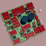
Some updates...
- Parametric EQs instead of notches
- Ballanced/regular input
- Ability to reroute the sections as you wish
- Jumper for 3-way/2-way operation
- Built-in traces for default 2-way/3-way configurations
- Onboard PSU with LM337/317 regs, propertly implemented (i hope so), with huge caps on output (can accomodate 10,000uf caps).
- Redesigned the whole layout of everything
- Had to go back to 2 SMT resistors instead of 4 in configurable places - still, you can stack-up the SMT resistors to get the right resistance.
- The "global" EQ with reroutinc could be used as fourth EQ at output...
That gives us ability to make... well, 5-way crossover
- I like the Altium's feature of "rounded" traces - they look way better on PCB.
Drawbacks... Well, i can't find a place to put the mounting holes...
Attachments
Some updates...
- Parametric EQs instead of notches
- Ballanced/regular input
- Ability to reroute the sections as you wish
- Jumper for 3-way/2-way operation
- Built-in traces for default 2-way/3-way configurations
- Onboard PSU with LM337/317 regs, propertly implemented (i hope so), with huge caps on output (can accomodate 10,000uf caps).
- Redesigned the whole layout of everything
- Had to go back to 2 SMT resistors instead of 4 in configurable places - still, you can stack-up the SMT resistors to get the right resistance.
- The "global" EQ with reroutinc could be used as fourth EQ at output...
That gives us ability to make... well, 5-way crossover
- I like the Altium's feature of "rounded" traces - they look way better on PCB.
Drawbacks... Well, i can't find a place to put the mounting holes...
Your approach shows a lot of potential. Here are some comments:
1. Power supply - I am not sure why you have such large caps on the output of the regulators. When the board is powered down, the supply side voltage will collapse before the caps on the output drain, so you will need to use the protection diodes as shown in the LM317 datasheet. If not, you risk damage to the ICs. The DC is already REGULATED. It's not like the caps on a power supply. You only need enough capacitance on the output to stabilize the regulator IC, as little as 10uF. If you use a value under 25uF, you don't need the protection diodes.
Also, you might want to move the voltage regulators to the edge of the board and allow room for the addition of a heat sink to each.
2. It's nice that you included a delay stage. Unfortunately, a single first order section for delay is extremely limited in what it can do. What is really needed is flat delay throughout the crossover region, especially above the crossover frequency. Typically you need multiple second order stages to accomplish this except for the lowest crossover frequencies, because the amount of delay that you can achieve by a single stage for all-pass corner frequencies of a couple of kHz (this is minimum) is too small. Can you make it possible to use multiple all-pass stages?
3. Will the board come assembled? If not, I think that the SMD resistors (and there seems to be a lot of them) are difficult for a DIYer to solder on without some advanced tools/skills. If the board is pre-assembled, how does one change the crossover frequencies and other components/parameters?
4. Without mounting holes, and with components right up to the edge all around, how would one actually mount/use the board? It can't just hover in place!
-Charlie
Thanks for feedback!
1. the "huge" caps are there for a reason. I've used a resistor in series with regulator to detach it's output from the board's supply.
Here is why:
- Regulators don't like big caps on their outputs
- Output impedance of refulator is curvy, frequency dependant...
- The regulator has slow reaction to voltage surges at input, therefore it's PSRR/rejection worsens as the frequency of noise at it's input rises. The C-R-C filter on reg's output cuts all the noise that have passed the regulator.
The regs are there to "charge" the large caps with constant voltage.
The "bypass" resistor should limit reverse current flowing thru regulator backwards on shutdown... but i'll add the diodes too, there is a space for them.
2. I agree on this point. The problem is board space, there isn't much space to put 8 stages (4 opamps) (which are sufficient for regular filter instances for correction of woofer-midrange offset).
The way i think of it is
- the All-pass section can be tuned low, and therefore give a larger delay, but gonna add some phase shift in driver's passband. The all-pass filters are there to fine-tune the phase alignment of drivers in both physical and electonic phase response. They couldn't be coherent, but their phase should match around crossover frequency to give a nice "null" on frequency resonse when one of the drivers is being connected in reverse polarity.
I need to investigate this theory in advance...
3. No, the board will be "bare". If you look closely, all the SMT components have "advanced" footprints which have regular thru-hole pads too. It's up to you to decide which components you'll use.
4. Yeah... i know... it's bad... but these holes are almost 8mm in size! As much as single opamp I'll search the way to squeeze them. at least 3 in count...
I'm limited in board size, as i want them cheap, and there is limit 100x100mm for each board in company i plan to order from.
There are electrolytic power supply caps under each opamp - you could use them as "standoffs"
1. the "huge" caps are there for a reason. I've used a resistor in series with regulator to detach it's output from the board's supply.
Here is why:
- Regulators don't like big caps on their outputs
- Output impedance of refulator is curvy, frequency dependant...
- The regulator has slow reaction to voltage surges at input, therefore it's PSRR/rejection worsens as the frequency of noise at it's input rises. The C-R-C filter on reg's output cuts all the noise that have passed the regulator.
The regs are there to "charge" the large caps with constant voltage.
The "bypass" resistor should limit reverse current flowing thru regulator backwards on shutdown... but i'll add the diodes too, there is a space for them.
2. I agree on this point. The problem is board space, there isn't much space to put 8 stages (4 opamps) (which are sufficient for regular filter instances for correction of woofer-midrange offset).
The way i think of it is
- the All-pass section can be tuned low, and therefore give a larger delay, but gonna add some phase shift in driver's passband. The all-pass filters are there to fine-tune the phase alignment of drivers in both physical and electonic phase response. They couldn't be coherent, but their phase should match around crossover frequency to give a nice "null" on frequency resonse when one of the drivers is being connected in reverse polarity.
I need to investigate this theory in advance...
3. No, the board will be "bare". If you look closely, all the SMT components have "advanced" footprints which have regular thru-hole pads too. It's up to you to decide which components you'll use.
4. Yeah... i know... it's bad... but these holes are almost 8mm in size! As much as single opamp
I'll search the way to squeeze them. at least 3 in count...I'm limited in board size, as i want them cheap, and there is limit 100x100mm for each board in company i plan to order from.
There are electrolytic power supply caps under each opamp - you could use them as "standoffs"
Ah, about the heatsink space and placement of PSU at the edge.
When i put the PSU in center, i get short and equal lengh traces to all of the components, and as a plus - the "star" topology power supply, where is no interference between power supply traces of each opamp. I think it is a good decision
Even the star ground is possible, but i doubt it will be better than double-sided pours. I can slice the layers to create it.
Last edited:
I'm interested to know what selections of SMD resistors you're designing around. In my research there only seems to be one type of thin film commonly around that is actually economical to use but it's not stackable.
I suppose they're not that expensive if I can put together a bulk order with other items.
I suppose they're not that expensive if I can put together a bulk order with other items.
Last edited:
Thick film are cheap and common. Could be bought over ebay for 100$ for whole E24 values set, 100pcs for each value.
20pcs/value goes for 16$ (don't know whether it's thick or thin film, but the price tells us it's thick)
170 Values 0805 SMD Chip Resistor COMPLETE Kit (0R~10M) - eBay (item 170470904131 end time Feb-03-11 15:01:03 PST)
Thin film are pricey.
Could you share yours thin film resistors source?
Thanks.
20pcs/value goes for 16$ (don't know whether it's thick or thin film, but the price tells us it's thick)
170 Values 0805 SMD Chip Resistor COMPLETE Kit (0R~10M) - eBay (item 170470904131 end time Feb-03-11 15:01:03 PST)
Thin film are pricey.
Could you share yours thin film resistors source?
Thanks.
- Status
- This old topic is closed. If you want to reopen this topic, contact a moderator using the "Report Post" button.
- Home
- Source & Line
- Analog Line Level
- XO3: The 1/2/3-way Active Crossover/filter PCB. Design suggestions welcome!