I'm sorry , I could not resist ... (below 1)
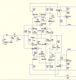
I kept the leach classic VAS and biased it to 4.8ma.
I kept the zener referenced cascode ,but balanced it.
I added ... 2 red led CCS's powered from the zener's
-running the LTP's at 4+ ma (similar to the good dr.)
It does 10ppm 1k -40ppm 20k , it has low open loop gain.
reducing the 300R LTP re to 100R really gave it a "kick in the butt"...
68R might be better.
EXtreme stability with my EF3 - performs real close to the CFA VSSA .")
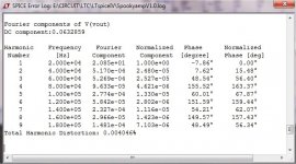
(below 2 ) 2/3 power 3R thd20...
I kept the leach classic VAS and biased it to 4.8ma.
I kept the zener referenced cascode ,but balanced it.
I added ... 2 red led CCS's powered from the zener's
-running the LTP's at 4+ ma (similar to the good dr.)
It does 10ppm 1k -40ppm 20k , it has low open loop gain.
reducing the 300R LTP re to 100R really gave it a "kick in the butt"...
68R might be better.
EXtreme stability with my EF3 - performs real close to the CFA VSSA .
(below 2 ) 2/3 power 3R thd20...
Attachments
You'd mentioned an attenuator or other circuitry to limit overdriving the amp. Implement it balanced and save balanced to single ended conversion.
Ha, yes, I didn't think of it as an attenuator, but that's what it is really. Sure, that's one way to go.
No, the 40V string keeps the input differential at 39.4V, then you've got the balance of the rail voltage to take care of. Take a look at the Honey Badger - it is cascoded on both legs of the differential and uses ~15V cascode reference to keep the input pair at 14V and then something else above. As Pass says in the F5T article, cascode transistors don't need to do much other than not break. In practice they are level shifters. In the Leach one side of the differential isn't cascoded, but the load resistor manages the voltage protection.
I see, well as long as we can make use of the high gain low noise parts, that's all good. Being able to use the bc550/60 instead of those mpsa42/92 or 2n5401/5551 should make a nice difference.
As far as having balanced inputs, it is best to keep that as a circuit separate from the PA feedback loop, especially if you want low-THD/TIM.
You've got a point there. Building a low tim and doing things that would defeat the low tim feature isn't good.
The whole TIM issue has been pretty much torn apart and relevant facts determined. Basically, anything that reduces THD20 reduces any risk of slew-induced effects. Input stage degeneration is all you need to be able to avoid TIM otherwise
If that's as simple as that, it's a good thing.
Does THD20 refer to 20hz or 20khz?
As long as you stay away from Miller compensation, then slew rate will be independent from the compensation itself.
But the leach amp uses miller among other things...
Device matching is the best (and hardest) path to achieving the lowest THD in any fully symmetric circuit. Most builders do not want to take the time to match, despite tonnes of evidence of its benefit.
That is my main goal in part selection. I have a plan to build as part tester as well, with nice features, so good and convenient matching can be done and a testing for second breakdown (non destructive of course) can also be done.
I like the massive heat sinks and such like of the chassis, but believe you are building a service nightmare that will have difficulties to construct as well.
I wanted to overbuild, especially on the heatsink, so heat would never be an issue and abuse would no change that.
I also have some ideas for an other "set" of amps where I want cooling tunnels with forced and regulated ventilation. That's a "set" because it's for a 4 way system, and I want all the amps in a single case, on wheels, because it will be very heavy with the multiple big toroids.
Consider the narrowness of each PCB and the "canyon" you have to work within to bolt the output transistor carriers onto the heat sinks. A friend of mine used allen-head bolts and a ball-end tool, claiming good off-axis access to the bolts. I found allen-heads easy to strip.
Each amp in the case being a module, it can be removed from it. And it's true that is a rather narrow pathway between the sinks. I had considered bringing the pcb higher, to make the access easier, but then there is a reduction of efficiency in the lower part of the heatsinks, so I lowered the pcb.
To make servicing easier, once a module is out of the case, if there really is a need to access hard to reach areas in there, the heatsinks can be removed from the module, because they are attached to those square braces, so the square braces don't have to be taken apart from the power transistors. Thus when putting it back together, the only thing to be careful about is to redo the thermal grease properly. I didn't find an other way to have such a big heatsink, with the fins vertical for best natural convection, and be able to have so many TO3s on it. It had to be done with the square brackets, unfortunately, so that's an extra thermal junction to deal with, but then the sinks are so big, they compensate for the extra Rth inserted there.
Cascoding the VAS is problematic with respect to stability. If you want to gain about 10dB open-loop gain and reduce THD much more dramatically, use the EF-VAS - just two BJTs more than the basic design and entirely stable. The collectors of these BJTs should be decoupled.
Yes, that's a good idea. The first transistor in that vas could then be a high gain type, unless there is an issue with the vce0...
I didn't think about extra decoupling on the vas, but I'll keep that in mind. I had planned for decoupling on every power transistor, so adding a few is no problem.
Remember that you have to build this AND service it. The leads from the toroids under the boards should be long enough to provide service access.
The toroids come with leads of about 20-25cm in length, which should be just enough to reach the pcb. It's easy to unmount the toroid from the support plate and push it aside near the end of the module. That should make it fairly accessible.
Hard to think about every detail and get it all perfect. It's good to share and have many heads thinking about those things.
I see you corrected the XLR wiring in post-79.
Note that Eagle can't assure correctness of your connections. It will only assure the board and schematic match - to a point. It will not warn you if two traces cross that should not.
Yes, it has those design rules, but we can easily make something that's not right without violating them. Which makes the sharing more important, with many people verifying things.
12mil trace spacing only provides 100V spacing. If you are using higher than +/-40V rails spacing should be doubled to 25mil (0.025"). This assumes a solder mask is applied on both sides. Also, use at least 2-ounce copper.
I'll have to double check on that. But there is only so much we can do, the parts can't be spread apart too much to allow much higher clearance. Even with a double sided pcb, many traces need to pass between legs, and we don't want to make traces overly long and circulating all over the pcb too...
Not so easy compromises. I'll have to recheck things...
Did you look e-Amp from Bonsai's website?
I like his e-amp, and I would like to build one, however the smd parts are not for me, so I would have to rework how it's done to allow all through hole parts. I have other projects in the work right now, so that would be for much later.
I sim the IPS with Ostripper's 3EF and got 220V/uS
If you want VFA with high slew rate, symmetrical VAS is the way to go.
WoW!
Extreme!!!
Very interesting. I am likely to apply such improvements on mine.
I have the EF3 "solved" flatpack opposed PCB layout with the dual Vbe
no leads for the Vbe and just cm's of trace between Vbe pre/driver.
Can we make an initial version using the MJ15003/4? I planned making more after that one with such parts, but I'd like to use my existing stock of TO3s first.
I will make the different versions, they can all fit within the same footprint, in the same case, same heatsinks and everything. The only thing changing besides the pcb layout is how the transistors are put on the heatsink.
About to splice your IPS onto the 3-pair "slewmaster" EF3 ...
I'll show the results ...
I can't wait! Making a high performance leach, without having to make the super leach with so many parts.
The flat packs could be located on the pcb edges, so they bolt on the heatsink directly, and this would leave lots of pcb real estate for layout.
The heatsinks are so big and present all along the pcb, there is no problem fitting lots of flat packs on them.
I'd like to have the asc so I can see the simulations. Your thd results look super promising.
Hi Guys
The mechanical access I was referring to was not related to removal of the TO-3 mounting bracket, rather just the bracket to the heat sinks.
It is no problem to have all six TO-3's cooled by the same heat sink, and in some ways it is preferred. The TO-3s have 50C higher temp range than TO-264 and other flat packs, so the all-metal package is a good choice for robustness. Self reported that it is best to place the thermal track device on top of the TO-3 case as this part of the device cycles quicker than the rest - especially much faster than the large heat sink. If you look at older amps, you find the thermal switches mounted this way - specially designed to fit over the TO-3.
With flat packs, the plastic case actually thermal cycles very quickly despite not being a good heat conductor.
With the split output stage, two thermal tracks are required.
The MJE150xx family of TO-220 drivers is quite robust and ubiquitous. Each driver must be rated to handle the sum of both rails:
MJE15028 /29(p): rated 120Vce
MJE15030 /31(p): rated 150Vce
MJE15032 /33(p): rated 250Vce
MJE15034 /35(p): rated 350Vce
All exhibit 30MHZ+ Ft at typical driver currents.
There is debate as to whether drivers should be on their own heat sink or on the main heat sink - advantages and disadvantages both ways; mostly depends on the rest of the circuit. In the cross-coupled driver stage the drivers operate class-A and their temp variation is pretty low.
The flat packs are the current way to do things as TO-3s are being phased out by the manufacturers. You can still use a flat bar to interface the BJTs to the heat sink, allowing through holes centered between the fins for the bolts securing the two pieces, with spacing independent of that of the BJTs. The 20mm wide TO-264 can be spaced with cases touching, or with a small gap to account for manufacturing variations.
The convenience of the TO-3P/246 mounting as it may be applied to the driver is enticing. With the very fast output devices available many of the arguments against using the larger package fall away. Even the much larger base capacitance is bootstrapped in the EF although in absolute terms the smaller devices still "win" there.
One problem with the 1381/3503 pair is that most vendors do not carry them in the same gain ranges. These devices come in four gain ranges. mouser and Digikey sell the 1381 in the E ranmge (100-200) and the 3503 in the D range (60-120). hard to find matches this way. I blew my cookies and bought a large quantity of both in the D range. In complementary circuits it is important to get the gains of the circuit halves equal, which is partly why you see these devices cascoded with other parts that can be matched. Most sims use the 1381/3503 in the C gain range. Who sells those? What happens when betas are 2-4 times different? Sims are not real life... unless all of what we think is real is actually a simulation? It's great that many here can do those simulations, but there is no THD meter in the world that can measure what the sims claim to be able to output.
The Leach circuit has a benign distortion profile, which is why many people like it. Regardless of where the real THD falls, it is that profile that makes the difference.
Have fun
Kevin O'Connor
The mechanical access I was referring to was not related to removal of the TO-3 mounting bracket, rather just the bracket to the heat sinks.
It is no problem to have all six TO-3's cooled by the same heat sink, and in some ways it is preferred. The TO-3s have 50C higher temp range than TO-264 and other flat packs, so the all-metal package is a good choice for robustness. Self reported that it is best to place the thermal track device on top of the TO-3 case as this part of the device cycles quicker than the rest - especially much faster than the large heat sink. If you look at older amps, you find the thermal switches mounted this way - specially designed to fit over the TO-3.
With flat packs, the plastic case actually thermal cycles very quickly despite not being a good heat conductor.
With the split output stage, two thermal tracks are required.
The MJE150xx family of TO-220 drivers is quite robust and ubiquitous. Each driver must be rated to handle the sum of both rails:
MJE15028
/29(p): rated 120Vce MJE15030
/31(p): rated 150Vce MJE15032
/33(p): rated 250Vce MJE15034
/35(p): rated 350VceAll exhibit 30MHZ+ Ft at typical driver currents.
There is debate as to whether drivers should be on their own heat sink or on the main heat sink - advantages and disadvantages both ways; mostly depends on the rest of the circuit. In the cross-coupled driver stage the drivers operate class-A and their temp variation is pretty low.
The flat packs are the current way to do things as TO-3s are being phased out by the manufacturers. You can still use a flat bar to interface the BJTs to the heat sink, allowing through holes centered between the fins for the bolts securing the two pieces, with spacing independent of that of the BJTs. The 20mm wide TO-264 can be spaced with cases touching, or with a small gap to account for manufacturing variations.
The convenience of the TO-3P/246 mounting as it may be applied to the driver is enticing. With the very fast output devices available many of the arguments against using the larger package fall away. Even the much larger base capacitance is bootstrapped in the EF although in absolute terms the smaller devices still "win" there.
One problem with the 1381/3503 pair is that most vendors do not carry them in the same gain ranges. These devices come in four gain ranges. mouser and Digikey sell the 1381 in the E ranmge (100-200) and the 3503 in the D range (60-120). hard to find matches this way. I blew my cookies and bought a large quantity of both in the D range. In complementary circuits it is important to get the gains of the circuit halves equal, which is partly why you see these devices cascoded with other parts that can be matched. Most sims use the 1381/3503 in the C gain range. Who sells those? What happens when betas are 2-4 times different? Sims are not real life... unless all of what we think is real is actually a simulation? It's great that many here can do those simulations, but there is no THD meter in the world that can measure what the sims claim to be able to output.
The Leach circuit has a benign distortion profile, which is why many people like it. Regardless of where the real THD falls, it is that profile that makes the difference.
Have fun
Kevin O'Connor
Last edited:
Can we make an initial version using the MJ15003/4? I planned making more after that one with such parts, but I'd like to use my existing stock of TO3s first.
I will make the different versions, they can all fit within the same footprint, in the same case, same heatsinks and everything. The only thing changing besides the pcb layout is how the transistors are put on the heatsink.
I can't wait! Making a high performance leach, without having to make the super leach with so many parts.
The flat packs could be located on the pcb edges, so they bolt on the heatsink directly, and this would leave lots of pcb real estate for layout.
The heatsinks are so big and present all along the pcb, there is no problem fitting lots of flat packs on them.
I'd like to have the asc so I can see the simulations. Your thd results look super promising.
The original Leach .... is what it is
Back when the good Dr. designed it ,he only had low Ft devices and wanted to keep it simple.
- No enhanced beta VAS = Very easy to compensate/stable .... but the
gain margin at 20K is insufficient for <10ppm THD 20. 20hz - 10k is
a fine 20-30 ppm any load without enhancement.
- The Dr. chose to split the FB into LF/HF , the 21st century way is
to servo the DC (like my NAD cfa) and use the standard divider for NFB.
- The triple ... he relied on the low Ft of his chosen devices. No decoupling
of the driver/predriver , or C-B shunts required. Ft of the devices won't
allow for that dreaded 10mhz oscillation (where most modern EF BJT stages
oscillate - without "tweaks").
BTW- MJ15003 To-3's are roughly equivalent to MJL21193/4 (low Ft/hfe).
I've had both sim/real world success with them ... MJ's would be perfect.
Below is .asc +text - plug your MJ's in for OP. This amp is rock solid.
PS - you could "ditch" the servo and just trim one of the led CCS's for
mV offset - keep it simple!
OS
Attachments
The mechanical access I was referring to was not related to removal of the TO-3 mounting bracket, rather just the bracket to the heat sinks.
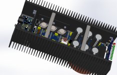
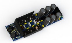
I'm posting a picture of the amp module, the version with the vu-meter.
Are you concerned about those 3 hex head socket screws mounting the square bracket on the heatsink? It would require an allen wrench, a long one might be better.
Do you have ideas to make this better? I'm open to suggestions.
It is no problem to have all six TO-3's cooled by the same heat sink, and in some ways it is preferred.
Sure, that's how it's done most of the time, with only one heatsink on one side. I just wanted more heatsink and possibly be able to make a single case from a module instead of a stereo amp. This works out well mechanically, however it's true the drawback is that it does separate the outputs in half.
all-metal package is a good choice for robustness. Self reported that it is best to place the thermal track device on top of the TO-3 case as this part of the device cycles quicker than the rest - especially much faster than the large heat sink.
I did want robustness, however I do have plans for later versions with the flatpacks. I was even seriously interested in those ThermalTrak parts, but their future seems rather uncertain and I hesitate on that. They would be great, the bias spreader could be a single small signal transistor, not needing to be mounted on the heatsink and the fact that the heatsinks are split would not be a problem that way.
With the split output stage, two thermal tracks are required.
We can arrange that. A couple of TO126 can be put together into a bias spreader.
ostripper is working on something to improve the leach. I think he's really on to something, and he can drop in a dual transistor bias spreader so we can put one on each side.
The MJE150xx family of TO-220 drivers is quite robust and ubiquitous. Each driver must be rated to handle the sum of both rails:
MJE15028
MJE15030
MJE15032
MJE15034
For this current version, the rails are planned at 61V, so the 30/31 would theoretically suffice, but I've seen improvements with the 32/33 in simulations, however that could be due to the models, or just because they have higher gain.
There are other things to consider besides their vce0 though, their current handling is half for the higher vce0 34/35 types. Although they do have the higher gain, the 4amps might be a little light when using many pairs of outputs.
There is debate as to whether drivers should be on their own heat sink or on the main heat sink - advantages and disadvantages both ways; mostly depends on the rest of the circuit. In the cross-coupled driver stage the drivers operate class-A and their temp variation is pretty low.
I favor the single heatsink as much as possible, however you can see that I opted for a smaller sink for the TO126 vas and pre-drivers, so I suppose the TO220s could be moved to that smaller one.
The TO126 bias spreader is fairly close to a TO3, but it is true that although somewhat close, there are 2 mica isolators plus the heatsink bracket to go through. The mounting is rather neat that way, and mounting the TO126 on top of the TO3 would be a bit tricky, as it would not have a complete surface contact with the TO3 and then there is an issue with wires. But if this is really a minus, I guess we can rework that.
I think there will be some good changes from what ostripper is working on, so we will revisit all this and look for better solutions.
It's still a work in progress and nothing is sculpted in stone.
the manufacturers. You can still use a flat bar to interface the BJTs to the heat sink, allowing through holes centered between the fins for the bolts securing the two pieces, with spacing independent of that of the BJTs.
I have trouble picturing this, but I think this might be a bit difficult without some machining on the heatsinks. The ones I use are standard from Fischer Elektroniks in germany. All they need is proper drilling and tapping for the screws.
Can you describe this more?
One problem with the 1381/3503 pair is that most vendors do not carry them in the same gain ranges. These devices come in four gain ranges. mouser and Digikey sell the 1381 in the E ranmge (100-200) and the 3503 in the D range (60-120). hard to find matches this way.
If I make use of those types, I would be inclined in using the KSA/KSC from fairchild.
I try to avoid the japanese ones, as they're often harder to get depending on where we are.
I blew my cookies and bought a large quantity of both in the D range. In complementary circuits it is important to get the gains of the circuit halves equal,
I want to do the best matching possible, and I know I will have to acquire big bunches of them to get good matches.
Attachments
21'st Century "Leach" ...
Interesting that the basic topology has not changed much.
HK's 990 (3000$usd) , uses the EXACT same IP pairs with/ Re as the original.
They augmented this with a beta enhanced Hawksford VAS.
All smd except for the toshiba sc4793/sa1837 as main VAS cascode.
This amp is near PPM (.005%/ 20k - full power). 2Q CCS is needed to
offset the enhanced beta VAS.The Led CCS is perfect for un- enhanced "plain"
VAS's.
I will use HK's servo , but really don't see the need to go "hawksford".
PS - 16V IP cascodes are fed from EF zener regulators and the IPS/
predrivers are fed from a 80V decoupled "boosted" supply. I
repaired this amp (and auditioned it ) - I DON'T own it . Spectacular !!
OS
Interesting that the basic topology has not changed much.
HK's 990 (3000$usd) , uses the EXACT same IP pairs with/ Re as the original.
They augmented this with a beta enhanced Hawksford VAS.
All smd except for the toshiba sc4793/sa1837 as main VAS cascode.
This amp is near PPM (.005%/ 20k - full power). 2Q CCS is needed to
offset the enhanced beta VAS.The Led CCS is perfect for un- enhanced "plain"
VAS's.
I will use HK's servo , but really don't see the need to go "hawksford".
PS - 16V IP cascodes are fed from EF zener regulators and the IPS/
predrivers are fed from a 80V decoupled "boosted" supply. I
repaired this amp (and auditioned it ) - I DON'T own it
. Spectacular !! OS
Attachments
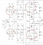
Hi Guys
OS, circled in red are REAL current sources. Most other things called CCS are not as good. Nice side-step of the 1381/3503 gain issue...
Spookydd, The flat interface for TO-3Ps to the heat sink is just that - a flat piece of aluminum bolted flat onto the heat sink. Those holes can be aligned with the heat sink fin spaces.
Meanwhile, the mounting holes and spacing for the TO-3Ps is completely independent of the fin spacing, so can be be set regardless of the heat sink used.
Although chassis symmetry is nice, you can make a single channel amp with one heat sink on one side. Look at the old Quad amps that had a heat sink on the front.
Most updates to Leach's circuit have been made over and over, so there's not much new to do - just people for whom it is new to them. You can pick whichever you wish to incorporate, or build it as originally laid out. You can read the old exchanges that ML had with his students and other builders/hobbyists, regarding heat issues using split heat sinks and such like.
With +/-60V rails, you are targeting 150W/ch at 8R, maybe 300W into 4R? This is optimistic, but a single heat sink will likely do the job. Do you know the thermal resistance for the one selected? or is there any data? I believe the middle heat sinks will be problematic.
Have fun
Kevin O'Connor
Hi Guys
...
Most updates to Leach's circuit have been made over and over, so there's not much new to do - just people for whom it is new to them. You can pick whichever you wish to incorporate, or build it as originally laid out. You can read the old exchanges that ML had with his students and other builders/hobbyists, regarding heat issues using split heat sinks and such like.
...
Have fun
Kevin O'Connor
I made an unique mod, replaced the 40V zeners with a shunt psu.
What it does...You have to construct it and hear for yourself.
Gajanan Phadte
Spookydd, The flat interface for TO-3Ps to the heat sink is just that - a flat piece of aluminum bolted flat onto the heat sink. Those holes can be aligned with the heat sink fin spaces.
Meanwhile, the mounting holes and spacing for the TO-3Ps is completely independent of the fin spacing, so can be be set regardless of the heat sink used.
That heatsink is rather thick at its base (over 9mm) and I didn't find it necessary to go all the way through. I make the holes tapped and blind, so the screws bolt right on the sink.
This could be done the same with any arrangement of plate and there is no need to even bother aligning with the fins. Makes it simpler.
Do you know the thermal resistance for the one selected? or is there any data?
Sure, of course. That sink is a standard one from Fischer, the SK479:
http://www.fischerelektronik.de/web_fischer/en_GB/heatsinks/A01/Standard%20extruded%20heatsinks/PR/SK479_/$productCard/dimensionParameters/index.xhtml
The length is 100mm, so according to their published Rth chart, we're slightly lower than 0.4K/W per sink. This is far more than enough for this build, and should also be quite sufficient for the subsequent and more powerful builds that I have planned.
I believe the middle heat sinks will be problematic.
In what way?
You're referring to the one used for the vas and pre-drivers I assume.
That sink is also a Fischer, standard, model SK546, in 50mm length.
http://www.fischerelektronik.de/web_fischer/en_GB/heatsinks/A01/Standard%20extruded%20heatsinks/PR/SK546_/$productCard/dimensionParameters/index.xhtml
From their chart, I read the Rth at about 3.75K/W for the 50mm length.
There isn't a very large amount of dissipation from the vas and pre-drivers. I figured this would be quite sufficient.
With +/-60V rails, you are targeting 150W/ch at 8R, maybe 300W into 4R?
The transformers I have on hand for this amp are 470VA toroids, with secondaries rated at 2x43V. Those don't sag very much under load, at least not below their rating at full power. Those specific toroids are a bit old now, as they're from the early 80s and from a now defunct manufacturer that had a reputation for the high quality.(metalimphy)
For the 8ohms load, they should hardly sag at all, and they'll do nicely for 4ohms.
Assuming they don't sag too much, the rails shouldn't drop much below 61V at full power, so I think that could allow some 38 or 39V rms on the load, accounting for various losses along the way. Maybe a little lower, but still that's more than 150W/8ohms, probably in the vicinity of 180.
I don't foresee any heatsink issues. I wanted to overbuild, for absolute robustness, all while aiming for all the quality we can get.
I had planned for 2 smaller heatsinks on the pcb, including one for the 2 rectifier bridges at the psu end of the board. That one is an SK597. All Fischer heatsinks.
This design will see some changes. The output relays and fuses will be replaced by SSRs for sure. The input will have an anti clipping limiter inserted there and I want to make it a muting at the same time.
The protection logic will be expanded to handle all this. And I am looking into protecting against shorts and overloads in an other way than the vi limiters. The anti clipping will serve well against overloads from the driving signal, and the heat sensing against long term over dissipation. Some other way besides vi limiters can be used to detect over currents and soa violations, and take appropriate actions other than shorting the drive from the drivers.
Attachments
By "middle" heat sinks I was referring to the sides of the modules in the middle of the chassis.
Ha, I see. You're concerned about proper convection compared to the outer sinks.
There is a good amount of space below, an open volume for air flow to go through, and the case is purposely full of holes for venting.
It's true it would tend to convect better on the outer than the inner sinks, but I preferred having 2 instead of just one. And I also planned to be able to use the modules to make a stand alone amp, mono, that would not be rack mountable as that big case is.
Hi Guys
Spookydd, you mentioned earlier about having some trace spacing issues, particularly with respect to the semi foot prints. I assume you know how to make your own library parts?
I use Eagle, as well, and have long since abandoned the stock library. For TO-92s I use a lead spacing of 100mil, inline not in a triangle, and a 32mil drill. I prefer to have large-ish pads for a proper amount of solder per connection, but for these use 'auto' sizing and there is voltage space of 318V between the pads. This easily allows running a 16mil trace between E and B when necessary.
Be careful not to make device footprints too small or too tightly packed together as you have to build this and later you'll have to service it.
Have fun
Kevin O'Connor
particularly with respect to the semi foot prints. I assume you know how to make your own library parts?
Sure, and I do a lot of the time, as there are always so many needed and not in the library. Plus the ones in the library have some issues.
TO-92s I use a lead spacing of 100mil, inline not in a triangle, and a 32mil drill. I prefer to have large-ish pads for a proper amount of solder per connection, but for these use 'auto' sizing and there is voltage space of 318V between the pads. This easily allows running a 16mil trace between E and B when necessary.
Do you really spread the legs of your TO92s that much?
This takes up a lot of space on the pcb too.
And if we want to keep that large of an isolation for everything, that means spacing parts as well all over the board.
Even Jens didn't do that on his leach clone boards.
Perhaps there is no need to go that far, with rails at around 60V, even with a little extra for comfort, we don't need a huge isolation.
Be careful not to make device footprints too small or too tightly packed together as you have to build this and later you'll have to service it.
That's true, and as impaired as I am, not even considering smd parts because I can't handle them, I need to think about my own abilities to manage the build.
I have a nice hakko soldering iron, with such thin tips, it could be used for smd easily, but that's a stretch for me. I love to solder and everything about electronics, but it's getting difficult for me now with small stuff.
Well, I'm posting everything I do as I get it done, so it's open to all scrutiny. Anyone can point out things that I overlooked.
Hi Guys
In the above TO-92 footprint I described, the space between the pads is 47.5mil (0.0475"). Using the 0.12mil/V guide for two-sided PCB with solder masks both sides, this provides 395V spacing.
Basically, in inches, take the space between pads/traces in mils (1mil = 0.001") and divide by 0.12 for volts. So, 12.5mil gives 104V.
Remember also that it is not jut the trace spacing that matters but also the space between the exposed solder "mountains".
I can't solder things spaced closer than 50mil and prefer larger spacings whenever possible. I try not to bend component leads right at the body, so leave a little more space between the ends of resistors, etc. I like inline lead spacing vs. triangular for TO-92s as it is much easier to insert the part..
If you hve 120V in your circuit you should not design for too close to 120V - how much margin is required vs. comfortable is anyone's guess. Everyone does whatever they have in mind regardless of advice up front. It's nice sometimes to avoid reworks.
Have fun
Kevin O'Connor
In the above TO-92 footprint I described, the space between the pads is 47.5mil (0.0475")
Well, that's more practical than 100mils.
And I suppose to bend the legs as well on the TO126 and TO220s...
Basically, in inches, take the space between pads/traces in mils (1mil = 0.001") and divide by 0.12 for volts. So, 12.5mil gives 104V.
I work in metric, so I'll have to do some conversions to be able to judge.
But this seems to me workable if I have rails at 60V. Unless the rails themselves get anywhere close to each other, the rest doesn't get exposed to quite as much.
Even if I add a bit of extra for safety margin, rail ro rail at about 120V, using 140 or 150V as a goal, using 20mils isolation isn't too far off.
Remember also that it is not jut the trace spacing that matters but also the space between the exposed solder "mountains".
That would be mostly around the pads.
I can't solder things spaced closer than 50mil and prefer larger spacings whenever possible. I try not to bend component leads right at the body, so leave a little more space between the ends of resistors, etc. I like inline lead spacing vs. triangular for TO-92s as it is much easier to insert the part..
How do you handle the TO126/220s??
- Status
- This old topic is closed. If you want to reopen this topic, contact a moderator using the "Report Post" button.
- Home
- Amplifiers
- Solid State
- Work In Progress... Leach Based Amplifier