Small digression..
Went to a 'Metal Supermarket' shop the inmates happily cut Ali to my Amp Case design specs for Very affordable prices...20$ of ali for a case .. Recommended")
I now have 2 ..3" ali angles 10" long and 1/4" thick.. to form the sides/top of my Amp case. As the 60sq inches of surface each.. heatsinks for the pcbs.
My rudimentary calcs suggest that this is adequate .. given my 25v power supplies.
Will assemble and temp test. Easy enough to add fins IF, necessary
Went to a 'Metal Supermarket' shop the inmates happily cut Ali to my Amp Case design specs for Very affordable prices...20$ of ali for a case .. Recommended
I now have 2 ..3" ali angles 10" long and 1/4" thick.. to form the sides/top of my Amp case. As the 60sq inches of surface each.. heatsinks for the pcbs.
My rudimentary calcs suggest that this is adequate .. given my 25v power supplies.
Will assemble and temp test. Easy enough to add fins IF, necessary
chat72, you read 29V across each resistor individually? What is your supply voltage? That reading would suggest a short or near short somewhere, with 290mA of current flow. Can you attach a picture (or a couple) of good quality so we can visually look for potential errors? You have verified output MOSFET location and orientation and have them properly insulated from the heat sink? Are your VAS devices full plastic package or do they have a metal tab that requires insulators?
I'll send pictures. Voltage drop on each resistor is 29-30v. I use plastic VAS and both Mosfet are insulated, I check with meters and there is no short between all legs and heatsink. I'm pretty sure that I didn't mix the semiconductors up. I use 29-0-29 ac this would be 40-0-40dc rails.

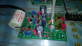

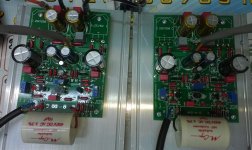
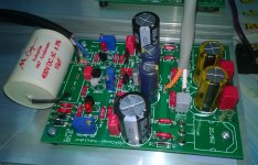
Better pics. I turn VR2 fully CW as suggeted so the bias should be minimum?
What's the measured resistance across the bias trimmer? LED's are lit?
Sheldon
Thanks Rick. The only issue is that image is for the default 2Q CCS, chat72 is using the 1Q+LED CCS. The general set-up sequence remains the same, just the values differ for the CCSs.
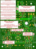
I suggested starting with the VR1 and VR3 adjusters at their max (1K) to minimize current. In reality I would start right at their mid-point assuming no issues.
@chat72 - what do you get across R13 and R14? I'm wondering if you have too much VAS current flowing which has everything turning on rather hard. Also verify Q1 and Q2 for proper orientation, just in case. I usually mark the top of one with paint prior to assembly so I don't get them mixed up (it happened once, now I usually mark the PNP device). What voltage are you getting across your LEDs?
Last edited:
Setting VR1 VR2 and VR3 to maximum and 120 ohms on the rails, I have around 1.5V across each ressitor so it about 12.5mA flow to the circuit. Voltage drop acroos both LEDs are 1.9V and I have 0V across R13 and R14.
Setting VR1 and VR3 to 600R, I have current around 90mA to the circuit.
V LEDS stays the same, V on R13 and R14 are 0.1V and I have DC offset at the output around 100mV (0.1V). Is DC offset to high? Both channels behave the same. Am I good to go?
Thank
Setting VR1 and VR3 to 600R, I have current around 90mA to the circuit.
V LEDS stays the same, V on R13 and R14 are 0.1V and I have DC offset at the output around 100mV (0.1V). Is DC offset to high? Both channels behave the same. Am I good to go?
Thank
Last edited:
Yes, start VR1 and VR3 at 500R or perhaps a little higher. Try to achieve 120mV to 160mV across R13 or R14 (12mA to 16mA VAS current) with the smallest DC offset possible. Then turn up the bias with VR2 to a total current of 120mA to 160mA depending on how good your heat sink is.
- Status
- This old topic is closed. If you want to reopen this topic, contact a moderator using the "Report Post" button.
- Home
- Amplifiers
- Solid State
- VSSA Through-Hole Version by Jason