Eh power is over rated anyway, better sound is my preference.
+1 to that. I can play my VSSAs louder than I can take for an extended session anyhow.
Jason,
Are you going to finish pcb from # 205?
Working on it. I don't get my layouts down quickly, I do a lot of ripping-up and re-doing, moving things around etc. to get it just so. Makes me slower than some of the forums more prolific artists. I'll post the 'new' version when it is ready, or at least really close for review. For now , a quick shot that is not complete. I'm just not sure when that will be.
First thing is to get the basic cap-x fully laid out and routed. Then I need to mess with the CCSs to see if I can do a layout offering either JFET and 1Q+LED types easily.
For the time being I do have revision 'C' boards for the existing circuit coming if you are interested in those.
Attachments
Last edited:
")
It looks like fun for comparing small signal transistors but 2.2mA max. base current seems a bit anemic for testing power transistors. I think you still need something simple and massive there.
They don't show you that part where you need a bigger regulated power supply and massive heatsink to stabilize the case temp. That's for you to work out, though.
They don't show you that part where you need a bigger regulated power supply and massive heatsink to stabilize the case temp. That's for you to work out, though.
Received my PCBs today Jason, they just look great! i will probably start stuffing them next week, as I still have to "curve trace" more transistors
THANK YOU!
Wow! You got your boards fast, certainly faster than I expected. Thanks for letting me know.
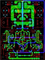
Low current CM in place, onto the CCSs
A quick snapshot with the CM on-board. Now time to mess with the CCSs, looking to see if I can integrate the 1Q+LED for those who like BJTs and the simple JFET for those who like that better.
Any other observations or suggestions are welcome...
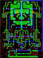
A quick snapshot with the CM on-board. Now time to mess with the CCSs, looking to see if I can integrate the 1Q+LED for those who like BJTs and the simple JFET for those who like that better.
Any other observations or suggestions are welcome...
Attachments
Hi Jason,
The layout as it's started now, provides the CM powered from the same power supply as the output stage.
A suggestion is to provide the option of a higher voltage supply for the input stage. For some people it might be unacceptable to lose headroom on the account of the MOSFETS added to voltage loss on the account of the cap multiplier.
I intend to build a stereo balanced amplifier using 4 of the received boards, but the input stage will be supplied from a shunt regulator. Thankfully the Resistor/diode group were still provided on board, so by not mounting them I don't need to hack the good looking PCB.
Cheers!
- Status
- This old topic is closed. If you want to reopen this topic, contact a moderator using the "Report Post" button.
- Home
- Amplifiers
- Solid State
- VSSA Through-Hole Version by Jason