......
Please don't ! It's a sin - like killing a unicorn...
Just take care not to feed them Vds before the Vgs is established. Otherwise they are pretty sturdy devices.
...don't want to do that for sure so i searched a bit and found that Michael Rothacher has published the measured curve... and the load line you chose fits the 2SK82 and 2SJ28 as well:
Attachments
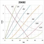
Yes i know Juma...the dashed line the picture i sent is 45W limit.
all i need to do is keep load line below that if i want to run the VFETs conservatively ( 50% rated power ).
Your devices have alimit of 63W, which you are running at 25 W, mine have a limit of 95W.
Did i get this right?
I wouldn't want to make a mistake...not with these.
Edit: the load line in my picture is the one MR chose for his aplication...not what i intend to use") .
.
all i need to do is keep load line below that if i want to run the VFETs conservatively ( 50% rated power ).
Your devices have alimit of 63W, which you are running at 25 W, mine have a limit of 95W.
Did i get this right?
I wouldn't want to make a mistake...not with these.
Edit: the load line in my picture is the one MR chose for his aplication...not what i intend to use
.
Last edited:


Edit: the load line in my picture is the one MR chose for his aplication...not what i intend to use
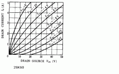
The item pictured is merely an example of a loadline from an article I wrote. It was not used in a project. Again, it's just an example.
why 51Volt to input ?
ahh, voltage doubler ?
why 51Volt to input ?
ahh, voltage doubler ?
It takes shear dumbness to realise the brilliance in Juma's amp.
You guys need more beer.

I am surprised how long it has taken for people to get interested in this one.
I set it up for Id=1A (25W dissipation per VFET) which gives about 32W_peak (16W avg.) in cl. A at 8 Ohms load but you can parallel more VFETs for lower bias per VFET and deeper into cl. A if you want. VFETS should belong to same Vgs/Id rank.
This power is good for me..
Finding Vfets with same rank is very difficult now....In the other thread you also suggested a schematic which has trimmers for adjustment...well, i think if that is good as this one then i think i will go in that one since my vFETS are not of the same rank..
why 51Volt to input ?
...To bias the VFETs properly I used the higher voltage rails for the input stage and EF. ...
A moderator that asks a question that's been answered in the first post of the thread... ts, ts, ts...
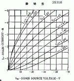
Look at the output char. of the VFET and you'll see that k60 needs it's gate at 10V lower potential than the source (and vice versa for j18). Since the source of k60 sits at -25V, the gate has to be at -35V so when we want the common source (drain follower) output stage it's only logical to use higher voltage rails in the front end (biasing) stage.
Last edited:
Sorry pico, some things still need changing, new version is on the way...
we're waiting.....
- Status
- This old topic is closed. If you want to reopen this topic, contact a moderator using the "Report Post" button.
- Home
- Amplifiers
- Pass Labs
- VFET PP amp