volts/day? or peanuts per hour?Slew Rate = 25.............
bimo
Please check what amount current is flowig threw the NFB resistors on full amplitude.
I will use 0,5W NFB resistor.
volt/year
Good answer! I always say that for the good listener... half a word...
Hmm, try a 22uF cap from emitter of ground. I suspect some of this bad behaviour at HF is due to the bias system.
Hugh
I will measure the exact votage between the base and gate of the output transistor and replace the bd140 transistor with few biasing diodes+resistor and increase the cap at the vas stage
BIG THX
GE,
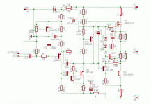
It's a modified CFP, using a R/C/diode all in paralleled between the master emitter and output to replace the pn junction of the driver, which of course is deleted with the upper nmos since its gate does not require a driver.
Since the inverting master and the nmos comprise the bias control, you need to soften the turnon of the master so that setting the bias is not too tetchy.
The diode is included so that when the lower output turns on the base current is high, and the diode prevents more than 0.6V dropped across the R/C/diode network. This is very important on a quasi since inserting the master costs rail voltage; you can't swing as much voltage at the output compared to a complementary output stage. This diode limits the loss of rail efficiency.
This phase inversion at the drive stage for a quasi is almost always used, many over decades. There are other ways, specifically to the JLH Class A very example, the advantage of this topology is that you combine a quasi drive with strong bias control at the output stage.
All electronic design is a mass of compromises......
Hugh
R18 could be any value from 330 to 100 ohms, depending on the type of transistor used for Q3. In my Quasimodo design, I use a 220ohm resistor and use a 2SB649A for Q3
I arrived at the value of R18 just by listening! I also use the 2SC5200 for the final transistor- a good combination, I find.
You just can't beat subjective listening tests as the final arbiter of finalizing an amp design.
Hugh has heard the Quasimodo, and will vouch for the validity of the last statement!
Christian's baby is going to be a good 'un, I think.
I'm off for a while now- I have yet another Quasimodo amp to build....and then another- It's all go here!
Hi Hugh
Still no sign of my boards I'm afraid; they must be on the slow boat from China - literally!
I'm about to pack the car and take the family up to Montville for a couple of nights away, followed by a short drive to Noosa, where my folks will be staying, to celebrate my father's 60th. Back to Brisbane on Saturday.
I'm hopeful the boards will be waiting on my return, in which case I'll waste no time assembling a prototype and conducting some listing tests, assuming it checks out on the bench.
I'll keep you posted...
Christian
Hi Hugh
Still no sign of my boards I'm afraid; they must be on the slow boat from China - literally!
Christian
I deal with China quite often for pcb's and get a very fast turnaround.
From order to receiving pcb's is usually 2 weeks.
They are always sent by a carrier so get here in about 3 days.
I also find Chinese pcb's to be about 1/3 the price of buying in UK.
I can get a set of Chinese pcb's for the cost of tooling in the UK.
Thanks Nigel.
I ordered mine from HQ PCB because Terry (aka still4given) indicated his positive experiences, and they had a simple online ordering interface. Communications have been excellent: order was placed 31/07 and goods despatched 6/08.
I try to support Australian companies and next time I'll enquire with some local suppliers and find out what they can offer.
There is small progress anyway. Today I have lowered the NFB resistor values to investigate the high freq artifacts, I have desoldered the bootstrap cap and all is ok.
I will put resistor in series with the bootstrap cap anyway.
AKSA
Could my problem be caused by the bias tranistor (my one is pnp bd140) emiter is directed to the not active side of VAS, should I change it with bd139 (emiter directed to the active side of VAS) ?
THX
I will put resistor in series with the bootstrap cap anyway.
AKSA
Could my problem be caused by the bias tranistor (my one is pnp bd140) emiter is directed to the not active side of VAS, should I change it with bd139 (emiter directed to the active side of VAS) ?
THX
Borys (Boris?)
Good question. I'm working from the schematic on #92, so I will use the designations on that schematic.
I don't think it makes any difference regardless if you use an npn or pnp; the AC path is via C6 which communicates very low impedance from Q4, an emitter follower, to BOTH gates.
I may be wrong because I do not use this Q2 bias system on the emitters of the input singleton, but I believe that the cause is a result of changing the impedances of the fb network wrt R15 3k3. I believe that changing R5/R6 dividers to LOWER impedances forces changes on the bias point. The current from Q2 which controls the offset supplies BOTH current into Q1 emitter AND R6, the series fb resistor. I think you need to make R15 relatively LOW wrt R6, and you also need to have a 47uF cap from emitter of Q2 to ground to hold this potential low. Actually, I believe this is a compromise though clever trick; my preference has always been to bias the base of Q1 via a 33K resistor, then ALL the current passing through Q1 is supplied entirely from the output node via R6.
I do not criticise this circuit. I think it is very clever and I'm very interested to hear the subjective tests. I know the THD will be high; particularly H2 and H4. This is not a purist, engineering design, but it will probably sound wonderful.
Cheers,
Hugh
Good question. I'm working from the schematic on #92, so I will use the designations on that schematic.
AKSA
Could my problem be caused by the bias tranistor (my one is pnp bd140) emiter is directed to the not active side of VAS, should I change it with bd139 (emiter directed to the active side of VAS) ?
THX
I don't think it makes any difference regardless if you use an npn or pnp; the AC path is via C6 which communicates very low impedance from Q4, an emitter follower, to BOTH gates.
I may be wrong because I do not use this Q2 bias system on the emitters of the input singleton, but I believe that the cause is a result of changing the impedances of the fb network wrt R15 3k3. I believe that changing R5/R6 dividers to LOWER impedances forces changes on the bias point. The current from Q2 which controls the offset supplies BOTH current into Q1 emitter AND R6, the series fb resistor. I think you need to make R15 relatively LOW wrt R6, and you also need to have a 47uF cap from emitter of Q2 to ground to hold this potential low. Actually, I believe this is a compromise though clever trick; my preference has always been to bias the base of Q1 via a 33K resistor, then ALL the current passing through Q1 is supplied entirely from the output node via R6.
I do not criticise this circuit. I think it is very clever and I'm very interested to hear the subjective tests. I know the THD will be high; particularly H2 and H4. This is not a purist, engineering design, but it will probably sound wonderful.
Cheers,
Hugh
AKSA
Thanks. I will try to do some modyficaions soon and post results. I do not care a lot about THD numbers anyway in this case. Amp was playing whole day without bootstrap capacitor, the sound is really smooth and nice. I have some spare time and basic tools, I have also lack of knowledge so any help is really gratefull.
THX Peter
Hi Christian,Thanks Nigel.
I ordered mine from HQ PCB because Terry (aka still4given) indicated his positive experiences, and they had a simple online ordering interface. Communications have been excellent: order was placed 31/07 and goods despatched 6/08.
I try to support Australian companies and next time I'll enquire with some local suppliers and find out what they can offer.
Sorry if I didn't make it clear that that the only thing I didn't like about them was that their "cheap" shipping option was a little slow. It usually take about three to four weeks to get them. I always think that won't matter but I always get anxious before they finally arrive. I'm waiting on some boards that Juan Vargas designed now. I ordered them on August 10 and they shipped on August 15th. It usually take about two weeks once they ship to get to me here in California. Not sure about Australia. Seemed like it took a long time for the package I sent to you to arrive there.
Blessings, Terry
- Home
- Amplifiers
- Solid State
- Very simple quasi complimentary MOSFET amplifier