quasi complementary that uses a FET and BJT !
The Big Advantage of using quasi complementray is that the upper and lower devices can be matched for all or most parameters.
When fed with a signal they both pass the same current.
When the signal changes they both follow, in opposite directions, their matched conductance curves.
That matching seems to be the reason that quasi complementary perform so well, even though looking at the sch, they are odd.
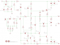
Gerbers finalised...
A few final tweaks and fixes and I've just now sent Gerber files off to the board house.
All going to plan I should have the boards in a few weeks. Once I've built a couple of prototypes I'll update this thread with the results and (fingers crossed) a listening report.
Thanks for your help everyone
A few final tweaks and fixes and I've just now sent Gerber files off to the board house.
All going to plan I should have the boards in a few weeks. Once I've built a couple of prototypes I'll update this thread with the results and (fingers crossed) a listening report.
Thanks for your help everyone
Attachments
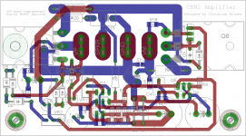
Thanks Hugh. I suppose I should invest in a quality prototyping board as a means of quickly testing my designs. That said, I do enjoy laying out the printed circuit as much as producing the schematic. There is also a financial outlay (albeit modest) in having the circuit boards manufactured, so I'm inclined to be discriminating of the ideas I pursue and more critical during the design process.
Parts values will be determined through listening experiments (note I didn't print them on the silkscreen!). I wonder how much negative feedback will be needed for good sound? I will probably spend a lot of time experimenting with different values for R10 and output bias points.
Parts values will be determined through listening experiments (note I didn't print them on the silkscreen!). I wonder how much negative feedback will be needed for good sound? I will probably spend a lot of time experimenting with different values for R10 and output bias points.
Ranchu32
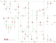
It really looks very interesting to me. Waiting for some feedback. I have all of the elements so maybe I will put it back together when I will have some time. Just make sure U will put D3 zener diode in the right dirrection on pcb board.
Could you explain me the temperature compensation mechanism ??
Hi borys, thanks for picking that up; I can't believe I overlooked something so obvious!
In terms of output biasing, I have it on good advice that the 0R47 source/emitter resistors will be sufficient to tame any tendency towards thermal runaway. However if this proves to be insufficient, one or more of the PCB mounted biasing diodes could be mounted on the heatsink for better thermal tracking.
The Vbe multiplier (Q2) to bias the input transistor is glued back-to-back with Q1 for better thermal tracking. This biasing scheme was designed by Bigun for his TGM8 project and works flawlessly. As a matter of fact, on Bigun's boards, the Vbe transistor is not in contact with the input, so if anything, thermal tracking should be improved with this layout.
RC,
I have just looked at the temperature compensation.
You may need five diodes, you will have around 5V bias from gate to base.
All will need to be thermally bonded to the output device, best on the mosfet. I would use a tab heatsink on T5 but not bond it to the output device heatsink.
I would increase the lag comp to 22pF (from experience) and add a phase lead across R21of 5pF.
To protect against EFI, I'd increase C2 to 1nF.
I'm still thinking about the tempco changes on Q2; I'd be using a zener there with a pot.
These are fine details. The topology is unique and will produce higher levels of distortion. THD will be around 0.02%, quite high, but dominated by H2/H4. This is not a purist amp, but it will be intensely musical.
Laying out a pcb takes a lot of time. There are lots of variations in your eye's mind. Having a few of them made will cost around $200 plus. You have to be absolutely sure that all component footprints are exact; a simple error will easily destroy a pcb and you can't use it. But it raises the stakes, and if you succeed your understanding of how electronics is manufactured reveals how hard but satisfying it really is.
Damn good work!
Hugh
Last edited:
Ranchu32
I have done some simulations at home and in spice the connection of the silver mica C4 cap is better on the lower part of the 330R resistor, directly to the q3 collector, with capactive loads C4 cap must be approx 47pF to keep the amp alive, some real life tests must be done anyway.
I have done some simulations at home and in spice the connection of the silver mica C4 cap is better on the lower part of the 330R resistor, directly to the q3 collector, with capactive loads C4 cap must be approx 47pF to keep the amp alive, some real life tests must be done anyway.
Thanks for your suggestions Hugh & borys.
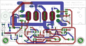
Unfortunately I have already sent the design in post #63 to the board house and it's too late to recall the order. The good news is that I should be able to accommodate most/all of the necessary changes with the existing layout.
I'll have a think about it over the weekend and update the schematic.
Unfortunately I have already sent the design in post #63 to the board house and it's too late to recall the order. The good news is that I should be able to accommodate most/all of the necessary changes with the existing layout.
I'll have a think about it over the weekend and update the schematic.

Ranchu32
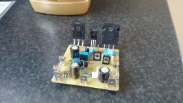
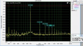
The good news is that the amp is playing very very nice, I am suprised really, just still have some clipping and square wave issues ( the lower part comming from BJT part of the amp) but it is interesting. There is a bit of work left on it anyway. Sorry for the 50Hz and up artefacts but there is some mess on my bench right now.
THX!!!
Attachments
BIT Thanks!!
I will post schematic and test board files evening time.Now I am at work.
The amp will play whole day anyway.
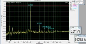
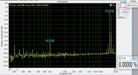
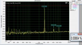
The bias looks stable ok. The clipping and square wave issues were caused by lack of current comming from AC ground 1mF capacitor, I have changed the NFB for 470/10k and square + clipping looks ok but thd rised obviously. The better AC ground must be prapobly developed or NFB bit changed cause it is consuming a lot of current.
It is suprisingly sounding very good.
I will post schematic and test board files evening time.Now I am at work.
The amp will play whole day anyway.
The bias looks stable ok. The clipping and square wave issues were caused by lack of current comming from AC ground 1mF capacitor, I have changed the NFB for 470/10k and square + clipping looks ok but thd rised obviously. The better AC ground must be prapobly developed or NFB bit changed cause it is consuming a lot of current.
It is suprisingly sounding very good.
Member
Joined 2009
Paid Member
keep up the progress and more reports about the sound please.
Bear in mind that to some extent you can tailor the sensitivity, or thermal gain, of the simple single transistor Vbe multiplier by changing resistor values to affect the split in current between two parallel paths. One path is through the transistor, the other through the resistors that set the bias at the base. With more current through the transistor it is more sensitive. If you want less sensitivity reduce the resistance of the bias string. I would expect the same is true when using a string of diodes for temperature compensation of the bias, you can put a resistor in parallel to a couple of them to fine tune.
Bear in mind that to some extent you can tailor the sensitivity, or thermal gain, of the simple single transistor Vbe multiplier by changing resistor values to affect the split in current between two parallel paths. One path is through the transistor, the other through the resistors that set the bias at the base. With more current through the transistor it is more sensitive. If you want less sensitivity reduce the resistance of the bias string. I would expect the same is true when using a string of diodes for temperature compensation of the bias, you can put a resistor in parallel to a couple of them to fine tune.
Last edited:
I can remain silent no longer!
Firstly, I must congratulate Ranchu32 for coming up with practically the same n- mosfet / p.n.p. transistor output stage as I stumbled upon around five years ago. It is virtually the same as that which I use in my Quasimodo design. And the clever fellow probably came up with it just by thinking "what if.....?!" as I did after first mucking about with a very blown up NAD310 around six years back.
I just cannot get away from that particular output combo as nothing sounds quite as "musical"- to my ears at least. Yes, the second and perhaps the fourth order distortion artifacts may be a little on the high side for some "meter jockeys" out there, but it sounds almost freakishly good as anyone who builds up Ranchu 32's little gem will find out. Although the front end stage on my Quasimodo design is rather different, a lot of that amp's "Magic" is due to the, let's face it, rather "whacky" n- mos / n.p.n. trannie output.
Funny, I thought that no one else would possibly come up with it- "too crazy" I thought- I wuz wrong!
I'm sure it will be a great success- I shall follow with great interest.
Cheers, All
- Home
- Amplifiers
- Solid State
- Very simple quasi complimentary MOSFET amplifier