Quick question.. Can the output grounds of the chips be tied together here?
I would like to put a switch on the output and switch between the rear binding posts and a front panel headphone jack with resistors in series. But I am unsure if the three(3) terminal headphone jack is compatible wit hthe seperate chips. To my knowledge the chip output grd is equal to pwr ground but I wanted to check and be sure.
I would like to put a switch on the output and switch between the rear binding posts and a front panel headphone jack with resistors in series. But I am unsure if the three(3) terminal headphone jack is compatible wit hthe seperate chips. To my knowledge the chip output grd is equal to pwr ground but I wanted to check and be sure.


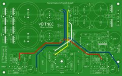
GeWa, do you mean that all the wires that you draw in your previous post have to be made with wire by hand? If so, good that this subject is on the forum. If not, i schould not know about it (the BOM do not speak about it too).
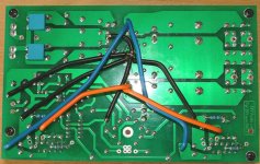
So for everyone who is going to build this amp, take good care off the photo from GeWa, a view posts ago.
So for everyone who is going to build this amp, take good care off the photo from GeWa, a view posts ago.
GeWa, do you mean that all the wires that you draw in your previous post have to be made with wire by hand?
Yes.
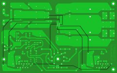
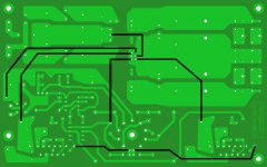
Also the HC and LC power supply has to be wired manualy. This is one of the disadvantages of a single layer board and the fact that it's only a euro card format (couldn't place the parts idealy). It all sounds a bit dramatically but it isn't. I will post a picture of how it all has to be wired.
Regards
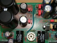
Attached a picture so you can see how the power supply wires have to be connected. For those who are interested, I slapped a small 3 page manual together which includes a parts list and some images and explanation of how to wire the amp. If you want one just send me an email. (to big in size to post it here, 375kb)
Regards
Regards
Attachments
Hello everybody. Well this is my first post to the forum. I've been watching this thread for some time as I liked the concept of the VBITNGC. I would like to give it a try myself.
Can I also get schematics and a manual, also files needed to make a pcb?
Thanks in advance.
Ah, yes, where can I get more information about the following:
Inverted configuration: In national's datasheet there's only noninverted conf described. How do I design things (formulas, etc) when I want to do it with Inverted topology? Where can I find resources for this?
T-Network: theory, why it works, calculations...
Is it possible to put 3875 in parallel mode? Resources? Schematics? Anybody tried it so far?
Uhhh.")
I hope I did not put so many questions in one post....
Can I also get schematics and a manual, also files needed to make a pcb?
Thanks in advance.
Ah, yes, where can I get more information about the following:
Inverted configuration: In national's datasheet there's only noninverted conf described. How do I design things (formulas, etc) when I want to do it with Inverted topology? Where can I find resources for this?
T-Network: theory, why it works, calculations...
Is it possible to put 3875 in parallel mode? Resources? Schematics? Anybody tried it so far?
Uhhh.
I hope I did not put so many questions in one post....
T-Network: theory, why it works, calculations...
Here, you will find everything about the t-network. In the first post, you can download an excel sheet for the needed calculations.
http://www.diyaudio.com/forums/showthread.php?s=&threadid=40664&highlight=
Kind regards
Franz
Franz, thank you very much for the link. Lots of very useful data.
Now, what is the present stage of the VBITNGC project? As I understand, there is a pcb that can be purchased but I dunno how. Also I am not quite sure of the full up to date schematics that is used for pcb. Can anyone post the full schematic please?
Also, is there any listening impresions of the project so far?
And yes, can I get files to make pcb myself? I mean, here in Belgrade we have nice small companies that make pcb's from files you bring'em on the disc. I believe that the pricing can be reasonable too.
My email is sir_john@bitsyu.net
Thanks everyone
Hi all - and you thought this thread was laid to rest!
Franz, if you are still listening - or anyone else! - I am finishing off a VBIGC based on Joe Rasmussen's schematic that I started building 2 years ago (yes, and I'm a slow house renovator too ). Point to point on perf board.
I'm thinking about the power-up delay. In your opinion, is it preferable to ground the input pin (8) on the LM3875 chip, or to switch the chip's power input?
Thanks!
Franz, if you are still listening
- or anyone else! - I am finishing off a VBIGC based on Joe Rasmussen's schematic that I started building 2 years ago (yes, and I'm a slow house renovator too ). Point to point on perf board.I'm thinking about the power-up delay. In your opinion, is it preferable to ground the input pin (8) on the LM3875 chip, or to switch the chip's power input?
Thanks!
- Status
- This old topic is closed. If you want to reopen this topic, contact a moderator using the "Report Post" button.
- Home
- Amplifiers
- Chip Amps
- VBITNGC building & comment