Using what i have on hand for measurements,i can't see something bad no at SA2015 not on the Slewmaster. Both aren't short path feedback devices.That capacitors has no big current spikes, as they are for the driver psu decoupling, and the feedback decoupling.
The lenght of the feedback path is the only difference? I mean that this is negligible amount of noise, and many things can change the result.
Sajti
Have a look here.SA2015 V-MOSFET Builders.post#14,17
Last edited:
Hi,
more than 10 pcs. of V4 was build, and basic configuration of the PCB was same since the beginning. The changes was only to adapt the output devices location for different heatsinks, and change some capacitor/resistor size.
All of them are working perfectly. But I like the challenge anyway, so I will give it a chance, and let me see if it will be better or not.
Sajti
Hi
8ppm at 128Wpk is pretty good for such a simple circuit. Excellent job, Sajti !!
When I do my circuit sims, I also check at the power levels I will actually use, which are very low, so 1W (way too loud 90dB), 100mW (still load 80dB) and lower. At these levels, if I can't get LTspice to show me all-zeroes (six zeroes after the decimal = <10ppb), then I'm not happy with the design. I suspect yours should show similar at least at 1kHz if not at 20kHz, too.
As far as the spacing between the PA input and the output go, this can be quite close even for a very-high-power amp where the output signal is 90Vpk. The key is in the grounding, as you already seem to know. For practical reasons, all the connections are on the rear panel of the chassis and the output stage is built along the side of the chassis. It is sensible to have the input stages on the rear apron of the chassis, or at least proximal, with the "noisey" power brought into the output stage card at its forward end or somewhere in the middle, in any event, distant from the input card.
In this very standard arrangement, it is easy to have power paths for DC and signal be well organised and separated. The main filter caps are close to the output stage as they should be and the input section is decoupled. By the time the output signal gets to the input stage area the signal is nothing but clean signal, i.e. it is fully summed into a whole sine wave. If you look at how most "super amps" (1kW+) are built, it is along this line and the inputs and outputs are closer together than one would expect.
Note that in amps with more space for everything, the main filter will be split into several caps per rail. This gives many advantages, one of which is in the basic layout of the current paths. In a simplistic approach, the caps would be in tow rails, one row per rail. The traces on the power end are a straight line from the bridge output, to the first cap, from first to second, from second to third, and so on. Similarly for the ground connection from the CT. The noisiest currents will be at the bridge-end of the cap group; the cleanest currents at the amp-end of the cap-group. Even though the entire cluster of caps contributes to handling the ripple and load currents, there is a measurable difference from one end to the other, so not purely aesthetic.
It is easy to configure the 3D arrangement of the PSU, the output stage, and the rear-panel board so that the electrical distance from the main filters to any output pair is quite short and that only "clean" power is presented.
")
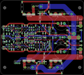

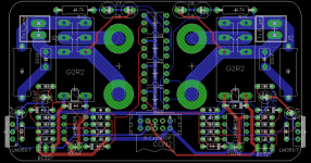
Your feedback path could be shortened if you place the feedback resistors in a line left from output. You could populate them vertical to save space.
The bias transistor has very long lines. To avoid oscillation you could add a 10R resistor to the base very close to the bias transistor.
Looks good so far!
Have fun,
Toni
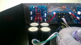
In my experiences, the most important thing for low noise / hum is the transformer distance from the pcb (also from input / output wiring / connectors, etc). Minimum 10 cm, more is better, or one can use some shielding method, like a belly band.
Attachments
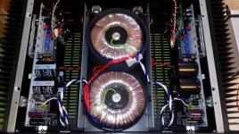
In my experiences, the most important thing for low noise / hum is the transformer distance from the pcb (also from input / output wiring / connectors, etc). Minimum 10 cm, more is better, or one can use some shielding method, like a belly band.
Where to by a belly band?
Thanks.
Where to by a belly band?
Thanks.
I made it myself. Take a toroidal transformer core and use some sheets (2-4) to form a band. easy
Last edited:
Your feedback path could be shortened if you place the feedback resistors in a line left from output. You could populate them vertical to save space.
I don't want to move the feedback network far away the star ground point. I use 3 different ground lines:
1, The feedback. It has relatively high AC current (about 30mA peak)
2, The compensation network at the VAS output
3, The input ground
This 3 route meet only at the star point.
The bias transistor has very long lines. To avoid oscillation you could add a 10R resistor to the base very close to the bias transistor.
It's not very long, and I never faced with oscillation, even when I used 10cm wire to the output device where the bias bjt was secured.
Sajti
The protection pcb was planned to support this binding post:
Dual Female Banana Plug Terminal Binding Post for Speaker Amplifier LW
Sajti
Dual Female Banana Plug Terminal Binding Post for Speaker Amplifier LW
Sajti
temp coeff. 450 ppm?
BR, Toni
Yes. But you will find no any problem with it. Output offset is few mV only, bias is stable.
Sajti
... OK - but what about extra noise?
This carbon film = 0.3µV/V noise
Metal film resistor: 0.0µV/V noise
BR, Toni
I hear no difference. Both the old, and the new amplifier is totally silent. No any noise of hiss even my with ear on the speaker.
My amplifier has the input sensitivity is 2Vrms for the full output.
Sajti
- Status
- This old topic is closed. If you want to reopen this topic, contact a moderator using the "Report Post" button.
- Home
- Amplifiers
- Solid State
- V6 amplifier