Indeed it is") It took some time to solder since manually applying the necessary amount of thermal paste is tricky. I had to retouch some of the pins a couple of times which is not nice. I prefer to get things right from the first attempt. But after two ICs I have better feeling of the process. I just hope I did not fry the chips
It took some time to solder since manually applying the necessary amount of thermal paste is tricky. I had to retouch some of the pins a couple of times which is not nice. I prefer to get things right from the first attempt. But after two ICs I have better feeling of the process. I just hope I did not fry the chips
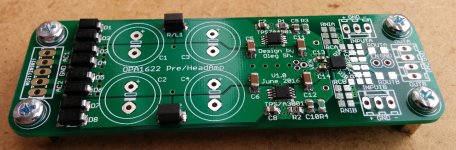
It took some time to solder since manually applying the necessary amount of thermal paste is tricky. I had to retouch some of the pins a couple of times which is not nice. I prefer to get things right from the first attempt. But after two ICs I have better feeling of the process. I just hope I did not fry the chipsAttached is the current state of my build.
Looks great!!!
One more question. As I wrote earlier I plan to use the OPA1622 in a single ended non-inverting configuration. To do so I planned to use 750 Ohm resistors to set the gain (2x) and input impedance in a similar way as it is shown in the datasheet which will result in 1k5 input impedance. I also plan to use a buffer before the OPA1622 to isolate it from the volume pot. So, may I safely assume that such a load is OK for an average op-amp/jfet based buffer?
Regards,
Oleg
Regards,
Oleg
To do so I planned to use 750 Ohm resistors to set the gain (2x) and input impedance in a similar way as it is shown in the datasheet which will result in 1k5 input impedance.
You should be OK. For one example NwAvGuy's O2 headphone amplifier the NJM2068 gain stage is driving a 10K pot and uses a 1.5K feedback resistor, which in the high gain case has a 274R resistor to ground. So the worst case load on the chip of 10K || (1.5K +0.274K) = 1.5K. The chip's datasheet has the THD numbers for a minimum of 2K load at 20dB gain and 5Vrms swing, so NwAvGuy must have figured close enough.
And that amp has been THD+N measured so it apparently worked out. Seems that a lot of the older opThe chip I would recommend tp buffer the (fet-input) OPA1622 is the FET-input OPA827, which is datasheet THD rated into a 600R load at G=+1 and a 3Vrms swing. The OPA827 is one of their newer generation chips that doesn't have the input-to-substrate voltage distortion issues the older FET chips did, and is much better about input series resistance distortion. The LME49720 and LME49990 (both bipolar) are also THD rated into 600R loads, G=+1, 3Vrms swing, but I believe TI is discontinuing both.
The OPA1688 may be another interesting choice as a buffer, but loop stability (on any of these) may be a question. In the OPA1688 CMOY project I have going on in another thread the V1.0 and V2.0 boards were set up where the OPA1688 could optionally power a plug-in OPA1622 on an adapter board. But I had forgotten to run Spice sims first.
The sim locks right up with the OPA1688 buffering the OPA1622 but works with the OPA827 as a buffer, as I recall. I assumed that was a stability/phase-margin issue but maybe just a sim artifact. At any rate something to look into.Good luck!
Hi agdr!
Thanks a lot for looking at my design! I also thought that 1k5 load should be OK since most of the newer op-amps are capable of driving 600 Ohm loads without increased distortion but I just wasn't confident enough. I guess I'll skip discrete JFET buffer option for now. I have a little stock of LME49720's so I may try it as the buffer. I can also try newer TI op-amps later.
BTW, I am following your OPA1688 CMOY thread with interest since the beginning. Very informative and inspiring!
Regards,
Oleg
I am back with another question. I'm slowly progressing with my build and just populated the input and feedback parts. The question is about ROUT(A/B). My situation is as follows. I have (and plan to have similar in the future) 32 Ohm headphones (Sennheiser HD428) with long cable (4~5m). Assuming cable capacitance is around 100 pF/m it could still be OK for OPA1622 without the output isolation resistor but it would be already near the border. So what would I lose performance wise if, for the peace of mind, I put 10 Ohm resistors at the outputs instead of zero Ohm jumpers? Or may be 5 Ohm resistors would be sufficient considering 5.5 Ohm output impedance of the OPA1622 itself?
Thanks,
Oleg
Thanks,
Oleg
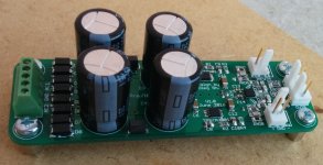
The board with the PSU is finished! The "enable" resistor divider (7k5 + 2k2 on the underside) is done such that the amp turns on at Vsupply > +4V and shuts down when Vsupply < +2.6 V. The PSU is configured for +-6V.
Now in order to listen to the headamp I have to partially disassemble my volume controller since I do not have another buffer lying around.
Regards,
Oleg
Now in order to listen to the headamp I have to partially disassemble my volume controller since I do not have another buffer lying around.
Regards,
Oleg
Attachments
Thanks phase!
I still have to try it. Regarding the Rout... I had my doubts and asked a question some days ago, but nobody commented on it so I had to decide by myself Since op-amp designer is very confident that in most cases Rout is not necessary I stay with zero Ohm jumper. If stability issues show up I'll change it to 10 Ohm later.
Regards,
Oleg
I still have to try it. Regarding the Rout... I had my doubts and asked a question some days ago, but nobody commented on it so I had to decide by myself
Since op-amp designer is very confident that in most cases Rout is not necessary I stay with zero Ohm jumper. If stability issues show up I'll change it to 10 Ohm later. Regards,
Oleg
I'm back to my hobby after the summer break
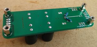
To AC couple the head amp I've designed a simple PCB (attached) which fits the capacitors with 5 to 20mm leads spacing with 2.5 mm steps. Originally the PCB was longer since I wanted to accommodate bigger polypropylene capacitors but after a bit of research I realized it is not really necessary and ended up with the current smaller board size (30x40 mm). The PCB can still accommodate the smaller 2.2 uF polypropylene caps which have a minimum pitch of 17.5mm and of course even smaller polyester caps. I plan to order a bunch of different caps (polypropylene, polyester) and try them in my headamp.
What's left is to decide which buffer to use after the volume control. So far I'm inclined to use LME49720 op-amp but am not fully set on it. Also is there a problem feeding the buffer and the head amp from the same regulated PSU? Is there a recommended arrangement, e.g. connect the head-amp straight to the PSU but use small series resistors (1~10 Ohm) to supply the buffer with local decoupling of 10~50uF // 100nF (making effectively a low-pass filter on the buffer supply line with the cut-off frequency below 1kHz where PSRR of the op-amp is typically high) or there is a better way?
Regards,
Oleg
Attachments
Have you looked at OPA1622 from Texas Instruments? This can directly drive 32ohm headphones. Has the ability to drive capacitive loads upto 600pF.
Sorry. Brain fart after midnight. Meant to refer to your thread on another forum. Posted in wrong tab.
Do the regulators have integral reverse biased diodes across each output to take care of momentary reversals if the two rails don't track during start up or shutdown? Didn't see those in your schematic.
You are driving balanced inputs with unbalanced signals. Do you think leaving the unused input floating is a good idea?
Also, might be a good idea to turn one of the input headers around, so the input cables are wired the same way. Someone might want to swap channels for testing, etc.
Last edited:
Hi SamAnytime,
Thanks for looking and your suggestions.
I thought of the reverse polarity protection diodes but searching around I've never seen them fitted to LDO regs designs even on the TI evaluation board. Whether they are inside of the regs package I can't tell, datasheet does not show them. Anyways, I can hardly imagine how reverse polarity can occur since there is no plan to drive inductive/switching loads by these regs. Also if one rail collapses/rises before the other the common GND should hold the regs ins and outs at the correct relative potential. May be I am wrong but so far I did not see a scenario where it can be a problem.
Well, what floats is one SMD pad, one connector pad and ~1 cm of trace between them. I doubt it will cause significant problem. The connector pad can be grounded on the underside of the PCB if this is required.
I guess potential user can turn the connector when assembling the board
Regards,
Oleg
Thanks for looking and your suggestions.
Do the regulators have integral reverse biased diodes across each output to take care of momentary reversals if the two rails don't track during start up or shutdown? Didn't see those in your schematic.
I thought of the reverse polarity protection diodes but searching around I've never seen them fitted to LDO regs designs even on the TI evaluation board. Whether they are inside of the regs package I can't tell, datasheet does not show them. Anyways, I can hardly imagine how reverse polarity can occur since there is no plan to drive inductive/switching loads by these regs. Also if one rail collapses/rises before the other the common GND should hold the regs ins and outs at the correct relative potential. May be I am wrong but so far I did not see a scenario where it can be a problem.
You are driving balanced inputs with unbalanced signals. Do you think leaving the unused input floating is a good idea?
Well, what floats is one SMD pad, one connector pad and ~1 cm of trace between them. I doubt it will cause significant problem. The connector pad can be grounded on the underside of the PCB if this is required.
Also, might be a good idea to turn one of the input headers around, so the input cables are wired the same way. Someone might want to swap channels for testing, etc.
I guess potential user can turn the connector when assembling the board
Regards,
Oleg
What does the opamp circuit look like with the -ve input floating? What resistance does the inverting input of the OPA1622 see to GND?Well, what floats is one SMD pad, one connector pad and ~1 cm of trace between them. I doubt it will cause significant problem. The connector pad can be grounded on the underside of the PCB if this is required.
- Status
- This old topic is closed. If you want to reopen this topic, contact a moderator using the "Report Post" button.
- Home
- Amplifiers
- Headphone Systems
- Universal buffer/headamp based on OPA1622