Guido Tent said:
My clocks' output impedance is about 10 ohm. Could you explain to the community why that can be considered a current source ?
Looks like I can only answer one question a day so I will do simple ones first.
")
When you reach the RF domain, often it's easier to analyze clock circuit by treating it as a curent source. It's more a matter of convenience. Basically clock is a current source charge/discharge into/from a capacitive load. You want a load impedance as low as possible so it can get the charge in the shortest period. In the meantime, the impedance can not be too low such that the voltage can not be transfered correctly. In Patrick's case, 45ohm is simply too low. Things will get much better if you make the load over 100ohm. If the clock is a pure voltage source, 100ohm will still be way too low, right?
To measure XO's output impedance is a very tricky job. The key is when you measure it? If the XO output driver is CMOS based, in the static mode, the output is either tied down to gound or tied up to power. Surely the output impedance will be very low at this moment. However, this is not what we are interested at. Instead, we want to look at it when it is doing the switches, i.e. the edges. This is the time a clock is doing the real job. Yep, not many instruments can do this. The best thing you can do is to measure the current surge rate, divide it by the voltage change rate to get some sort of pesudo output impedance. Still a very trick work to do.
Assume you have a CMOS inverter driver swtching the output from 1 to 0. As soon as the PMOS is turned off and NMOS is turned on, the output of the inverter will go down to ground very quickly. Then slowly, this ground point will draw current from the fanouts to pull everybody (those capacitive loads) down to ground. Obviously the initial voltage change is much faster than the current change, this will give the inverter a very high initial output impedance. This is why you prefer to treat clock as a current source.
KC7 is another interesting case. It uses a comparator as the output driver. Comparator usually has a strong current drive capability. For instance, AD8561 can output peak current as high as 40mA. This is enough to drive at least 10 TTL gates! Such a strong driving power makes overshot and undershot something unavoidable. Is this bad? Not really. Actually such a strong driving capability makes KC7 a more forgiving clock to use.
Talk about capacitive load. Definitely you want to keep it as low as possible. Too big a load will have bad ringing problem. As a general rule, try to keep it under 60pf.
-finney
Guido Tent said:
Hi Fin
Thanks for feedback and insight in 1704 architecture - very interesting (TDA1541 also consists of more DACs - it grew from an industrial 11 bit / 200kHz DAC, first they applied 8 in the TDA1540)
From what I read in the 1704 datasheet is that it converts on the BCK. I assume this is a straight wire from pin 2 right into silicon, not ?
Given the sonic results, I would be very much surprised if a PLL was inbetween.
The CS8412/14 PLL is not good enough for serious audio conversion. In addition, a secondary PLL could be added. I designed one and offer that as an add on module, see the TentLabs site.
cheers
Hi Guido
You hit the problem right at the nail! Anyway, I saw you had put in tremendous efforts in the past few years to educate people here about this. As a general rule, similar to yours, if the DAC chip needs system clock, I will always put in a reclocking circuit. Never use the SCK output from CS8414, etc, directly.
In most DAC chips, BCK will be buffered first then to drive the shift register which stores incoming bit data. WCK will dump the data in the shift register to another register then trigger the conversion process. The conversion goes in stages, just like a pipeline, controlled by the DLL. The DLL here is really just a fancy delay line. It should be totally transparent to the user and we do not have to worry about its jitter. From the clock input perspective, PCM1704, same as PCM63, 1702, etc, is as clean as you can get. Those new DACs which need SCK are nasty.
I honestly do not know how many DACs are inside PCM1704, but I do hear there are *many*, some of them in different sizes. Each DAC needs to be laser trimmed so the chip is very expensive to make. Another problem with PCM1704 is that there are so many DACs to be linked together through switches, the noises from the links and switches will hurt the resolution of the lowest several bits. This will set a limit to the highest dynamic range it can get. This is why everybody has switched to the multi-segment approach, as dCS (those guys are very very good!) forsaw years ago.
It will be great if you can find more info about TDA1541. I really want to know how that active current divider is done. Yes, it is of the transistor switch kind but any more info other than that? I believe the secret of 1541's good sound lies in this divider. Thanks.
-finney
The DLL here is really just a fancy delay line.
Hmmmm.........I suspected as much, based on your previous post.
I honestly do not know how many DACs are inside PCM1704, but I do hear there are *many*, some of them in different sizes.
So that explains why it draws so much current on the -5 rail, at least compared to a AD1862.
Which looks much better on the 'scope, when you look at the lowest bits. The MSB trim adjustment stays put on them. I have some from 12 years ago that are still exactly where they were back then.
OK, next question.............any idea what is inside the PCM1792????
Jocko
Monoticity
Interesting thread even though the content is a bit far away from the Threadname.. Maybee a new thread for the discussion of the internal layout of a DAC should be made ?
PCM1702 datasheet:
"increasing values of digital input will
always result in increasing values of DAC output as the
signal moves away from bipolar zero in one-LSB steps"
This indicates that Finneybear is right about he's claim that the dac contains more than two R2R dac's inside..
The datasheet of a 1704 DAC, dosn't tell anything about the monoticity but I expect it's the same here.
Archiving monoticity in a 19bit dac, is much harder than archiving it in, lets say 8*16bit dac's.
finneybear said:
Looks like I can only answer one question a day so I will do simple ones first.
When you reach the RF domain, often it's easier to analyze clock circuit by treating it as a curent source. It's more a matter of convenience. Basically clock is a current source charge/discharge into/from a capacitive load. You want a load impedance as low as possible so it can get the charge in the shortest period. In the meantime, the impedance can not be too low such that the voltage can not be transfered correctly. In Patrick's case, 45ohm is simply too low. Things will get much better if you make the load over 100ohm. If the clock is a pure voltage source, 100ohm will still be way too low, right?
To measure XO's output impedance is a very tricky job. The key is when you measure it? If the XO output driver is CMOS based, in the static mode, the output is either tied down to gound or tied up to power. Surely the output impedance will be very low at this moment. However, this is not what we are interested at. Instead, we want to look at it when it is doing the switches, i.e. the edges. This is the time a clock is doing the real job. Yep, not many instruments can do this. The best thing you can do is to measure the current surge rate, divide it by the voltage change rate to get some sort of pesudo output impedance. Still a very trick work to do.
Assume you have a CMOS inverter driver swtching the output from 1 to 0. As soon as the PMOS is turned off and NMOS is turned on, the output of the inverter will go down to ground very quickly. Then slowly, this ground point will draw current from the fanouts to pull everybody (those capacitive loads) down to ground. Obviously the initial voltage change is much faster than the current change, this will give the inverter a very high initial output impedance. This is why you prefer to treat clock as a current source.
KC7 is another interesting case. It uses a comparator as the output driver. Comparator usually has a strong current drive capability. For instance, AD8561 can output peak current as high as 40mA. This is enough to drive at least 10 TTL gates! Such a strong driving power makes overshot and undershot something unavoidable. Is this bad? Not really. Actually such a strong driving capability makes KC7 a more forgiving clock to use.
Talk about capacitive load. Definitely you want to keep it as low as possible. Too big a load will have bad ringing problem. As a general rule, try to keep it under 60pf.
-finney
Fin,
Keep it simple
In either end, it ios about 10 or 20 ohm. Then there is the cross conductance phase where simply put the impedanve halves.
In either case it is low, so it isn't a current source. The only aspect adding impedance is the series inductance in bond wiring, leadframes and PCB wiring. But still it isn't a current source.....
I reccomend loading a clock with the highest impedance possible in order to reduce charge transfer and density as much as possible.
Another aspect is the load termination, if required I prefer RC termination, but above all I even more prefere source termination. By doing so the source does not have to deliver power in the load termination......
Thanks by the way for all the insight info on the DAC chips discussed - helpfull.
best regards
Jocko Homo said:Hmmmm.........I suspected as much, based on your previous post.
Well, you are more than welcome to have the benefit of doubt. Sounds to me that you must have facilitated a better way to link all of those DACs together? Mind sharing the idea with us? Oh, the output settling time for PCM63, PCM1702, PCM1704 is all the same: 200ns, even when they are based in different processes, different geometry. Must be a coincidence with miracle in work?
Actually you can just check 1704's output with a good scope. Equiped with a decent spectrum analyzer is even better.
So that explains why it draws so much current on the -5 rail, at least compared to a AD1862.
Which looks much better on the 'scope, when you look at the lowest bits. The MSB trim adjustment stays put on them. I have some from 12 years ago that are still exactly where they were back then.
I bet that AD1862 will look better.
OK, next question.............any idea what is inside the PCM1792????
Y'right, so I will give you more benefit of doubt?
Be serious, can we talk about this some other time? Plus you have my email address anyway. I still need to find the time to discuss this stability thing, jitter, Allan deviation, etc. I could chat a bit more in the past few days because I was in between projects. Now a new project is about to start.
CS43122 is a good start point. Its datasheet is excellent. There are many publications and white paper available, too. Hell, even EE Times talked about it.
-finney
Re: Monoticity
Wow, I am impressed! Now I only wish every engineer in my company is as keen as you are! Not many people can read through lines in a datasheet and fully comprehand what they are talking about. Impressive!
Allow me to elaborate a bit more: The LSB bits are driving multiple DACs at the same time. So the higher those LSB bits go, the more current each DAC will generate. Now it is the highest MSB bits to decide which DAC's output current will reach the final chip output. Say, two DACs output will be blocked when the rest two will go to the final output. The problem here is that the switches to block the DAC outputs are far from perfect. It has current leakage. The higher the current goes, the more leakage it will have. Eventually this current leakage will reach the chip output. So the higher value the LSB bits have, the further the DAC output current will drift away. This is one of the main reasons why multibit DAC's dynamic range can't go higher.
-finney
Lgrau said:PCM1702 datasheet:
"increasing values of digital input will
always result in increasing values of DAC output as the
signal moves away from bipolar zero in one-LSB steps"
...
Archiving monoticity in a 19bit dac, is much harder than archiving it in, lets say 8*16bit dac's.
Wow, I am impressed! Now I only wish every engineer in my company is as keen as you are! Not many people can read through lines in a datasheet and fully comprehand what they are talking about. Impressive!
Allow me to elaborate a bit more: The LSB bits are driving multiple DACs at the same time. So the higher those LSB bits go, the more current each DAC will generate. Now it is the highest MSB bits to decide which DAC's output current will reach the final chip output. Say, two DACs output will be blocked when the rest two will go to the final output. The problem here is that the switches to block the DAC outputs are far from perfect. It has current leakage. The higher the current goes, the more leakage it will have. Eventually this current leakage will reach the chip output. So the higher value the LSB bits have, the further the DAC output current will drift away. This is one of the main reasons why multibit DAC's dynamic range can't go higher.
-finney
I have your e-mail address????
News to me...............guess my memory is getting worse.
As for datasheets......most of us have learned to ignore large portions of them. A lot is wrong, the good stuff is missing, and they give few clues as to what their weak points are.
And then there is the DIR1703 data sheet. Perhaps the only thing worse than the DIR1701.
Jocko
Guido Tent said:
Fin,
Keep it simple
In either end, it ios about 10 or 20 ohm. Then there is the cross conductance phase where simply put the impedanve halves.
In either case it is low, so it isn't a current source. The only aspect adding impedance is the series inductance in bond wiring, leadframes and PCB wiring. But still it isn't a current source.....
I reccomend loading a clock with the highest impedance possible in order to reduce charge transfer and density as much as possible.
Another aspect is the load termination, if required I prefer RC termination, but above all I even more prefere source termination. By doing so the source does not have to deliver power in the load termination......
Thanks by the way for all the insight info on the DAC chips discussed - helpfull.
best regards
Hi Guido
Let me keep it simple, too. Looks like your analysis is more based on the quiescent state when my focus is on the active region. Yet remember the main focus here is the shape of the waveform. Since you claim the larger load impedance the better, why don't you hook up your XO with a 100K ohm load and a 40pf cap in series to see how it goes? Why did you tell Patrick to add on a 50ohm resistor instead of a 10K one? BTW, many XO companies simply load the osc's output with a 15-30pf cap to do the testing. They must love to test the worst case scenario?
Talk about XO companies, Allan deviation is a widely adpoted measurement for stability test. It strikes odd to me that you are not familiar with Allan deviation but claim stability has nothing to do with jitter?
-finney
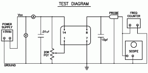
Attached diagram is a typical setup for XO test.
Attachments
Re: I have your e-mail address????
Yeah, this is surely the hardest part! We all have learned the hard lesson.
And yeah again, you do have my email address. Probably I am such an insignificant figure that my existence fails to get any traction in your vast memory. Just kidding!
Jocko Homo said:News to me...............guess my memory is getting worse.
As for datasheets......most of us have learned to ignore large portions of them. A lot is wrong, the good stuff is missing, and they give few clues as to what their weak points are.
Yeah, this is surely the hardest part! We all have learned the hard lesson.
And yeah again, you do have my email address. Probably I am such an insignificant figure that my existence fails to get any traction in your vast memory. Just kidding!
Jocko Homo said:Not insignificant.........just drawing a blank. It happens when your mind is preoccupied with digging up your sewer line. Don't ask about the sewer line from hell. Must have been designed by Bill Gates.
OK.......jog my memory and send me an e-mail.
Jocko
Hehehe... as usual, you have never lost your sense of humor! Will do. Later.
-finney
- Status
- This old topic is closed. If you want to reopen this topic, contact a moderator using the "Report Post" button.
- Home
- Source & Line
- Digital Source
- Undershoot in Kwak clock 7