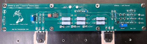
+1 UDNeSS
First channel adjusted (partially) and settled nicely but not quite sharing equally.
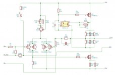
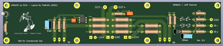
I used the Revision 2.0 revised schematics and was not quite clear on all the 'extra' resistor footprints (plus I omitted the servo) but now it makes more sense.
R11a (R112a on the board), R14a are used to 'tune' the current sharing between the 2 mosfets but you won't know what adjustment to make until you've got it running and measuring AC across R15/R16. I don't have either of these populated currently and I used the values straight from the schematic for Rev2.0.
R6 on the back of the board sets bias and there are 2 slots so you can parallel resistors (SMD). I just used the really small Panasonic 1/2W resistors here as I have a bunch of different values from back in the Peter Daniel (Aleph30) days.
I don't have the 2SK209 pcb so I just resorted to using 2SK170BL instead.
What I used
Fairchild FQA9P25 mosfets (thanks Dennis!)
J113 for Q1
2SK170BL for Q2/Q3 (Idss below 7.0mA)
100R for R6 (single)
For Rdg, I started with a 1K pot. When I first powered it up, there was no current going through R15 and I had 22V DC offset on the outputs. I thought maybe it was broken or I had incorrectly installed something but twiddling with Rdg brought offset down quite quickly and at the same time, current started flowing through R15.
I ended up with about 86R on Rdg and eventually swapped it for 100R pot instead of the 1K and let it warm up. It settled around 48C on the heatsink and Rdg measured 83R so I swapped in a fixed resistor at 82R. Now when it's warm, it hovers around 10mV of offset. Note that the offset cycles up and down through about 30mV. Current through R15/R16 was 682mV or 1.364A. Clamp meter agreed with this more or less (1.367A) although sometimes they differed by as much as 30-80mA. If I were to do this over, I would put 200R for R6 in parallel with a 500R pot. Based on the comments from Bullittstang, I suspect I'll probably need somewhere around 65-80R to get this channel down to 1.3A.
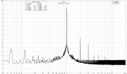
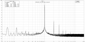
I don't know about the 2SK209 version but with the 2SK170BL, this thing has quite a bit of gain. Input voltage to get it to 1W (8Vp-p) with 1KHz sine wave was only 380mV. Heatsink is probably a bit smaller than the 3U/400mm and stabilizes at 48C, although it feels hotter than that (or my hands have become more sensitive).
It's definitely H2 (positive) and sounds really good in initial testing. Very lively in my limited testing.
I'll get the second channel running next and as long as it matches the first channel I don't think I will bother adjusting R11-14. Right now at 1W into 8R dummy load (single ended input, Vin- shorted to GND), I measure 137mV AC across R15. Seems like a lot of work to try and squeeze a 0.1R resistor between Q4 and V-. There is about 1-2C temperature differential between the 2 mosfets but this is just an exercise build for now (which explains the hack mounting - apologies if anyone is offended") )
)


Thanks to Patrick (EUVL) for a fun and educational exploration into a great sounding project that doesn't require difficult to find parts!
This particular implementation seems to be a bit contradictory in that the people who would be brave enough to take on the challenge of building it, probably have the parts to build something J2-like. I guess the question the builder needs to ask themself is are you looking for a J2 or are you looking to build a great sounding amp that match the publicly available specs of a J2?
Just for fun, I took the J2 (Toshiba 3467/SS version) schematic and compared it to the UDNeSS and it literally looks the same, except upside down. I haven't gone as far as comparing the actual footprint connections but if those match, you could plausibly use the same board for UDNeSS or J2!
What might be an interesting academic pursuit would be to see if there is the possibility of making a board that could be used for J2-like or UDNeSS or the simulated dual rail F8 using the same board ...
(@Dennis,

 )
)
First channel adjusted (partially) and settled nicely but not quite sharing equally.
I used the Revision 2.0 revised schematics and was not quite clear on all the 'extra' resistor footprints (plus I omitted the servo) but now it makes more sense.
R11a (R112a on the board), R14a are used to 'tune' the current sharing between the 2 mosfets but you won't know what adjustment to make until you've got it running and measuring AC across R15/R16. I don't have either of these populated currently and I used the values straight from the schematic for Rev2.0.
R6 on the back of the board sets bias and there are 2 slots so you can parallel resistors (SMD). I just used the really small Panasonic 1/2W resistors here as I have a bunch of different values from back in the Peter Daniel (Aleph30) days.
I don't have the 2SK209 pcb so I just resorted to using 2SK170BL instead.
What I used
Fairchild FQA9P25 mosfets (thanks Dennis!)
J113 for Q1
2SK170BL for Q2/Q3 (Idss below 7.0mA)
100R for R6 (single)
For Rdg, I started with a 1K pot. When I first powered it up, there was no current going through R15 and I had 22V DC offset on the outputs. I thought maybe it was broken or I had incorrectly installed something but twiddling with Rdg brought offset down quite quickly and at the same time, current started flowing through R15.
I ended up with about 86R on Rdg and eventually swapped it for 100R pot instead of the 1K and let it warm up. It settled around 48C on the heatsink and Rdg measured 83R so I swapped in a fixed resistor at 82R. Now when it's warm, it hovers around 10mV of offset. Note that the offset cycles up and down through about 30mV. Current through R15/R16 was 682mV or 1.364A. Clamp meter agreed with this more or less (1.367A) although sometimes they differed by as much as 30-80mA. If I were to do this over, I would put 200R for R6 in parallel with a 500R pot. Based on the comments from Bullittstang, I suspect I'll probably need somewhere around 65-80R to get this channel down to 1.3A.
I don't know about the 2SK209 version but with the 2SK170BL, this thing has quite a bit of gain. Input voltage to get it to 1W (8Vp-p) with 1KHz sine wave was only 380mV. Heatsink is probably a bit smaller than the 3U/400mm and stabilizes at 48C, although it feels hotter than that (or my hands have become more sensitive).
It's definitely H2 (positive) and sounds really good in initial testing. Very lively in my limited testing.
I'll get the second channel running next and as long as it matches the first channel I don't think I will bother adjusting R11-14. Right now at 1W into 8R dummy load (single ended input, Vin- shorted to GND), I measure 137mV AC across R15. Seems like a lot of work to try and squeeze a 0.1R resistor between Q4 and V-. There is about 1-2C temperature differential between the 2 mosfets but this is just an exercise build for now (which explains the hack mounting - apologies if anyone is offended
)
Thanks to Patrick (EUVL) for a fun and educational exploration into a great sounding project that doesn't require difficult to find parts!
This particular implementation seems to be a bit contradictory in that the people who would be brave enough to take on the challenge of building it, probably have the parts to build something J2-like. I guess the question the builder needs to ask themself is are you looking for a J2 or are you looking to build a great sounding amp that match the publicly available specs of a J2?
Just for fun, I took the J2 (Toshiba 3467/SS version) schematic and compared it to the UDNeSS and it literally looks the same, except upside down. I haven't gone as far as comparing the actual footprint connections but if those match, you could plausibly use the same board for UDNeSS or J2!
What might be an interesting academic pursuit would be to see if there is the possibility of making a board that could be used for J2-like or UDNeSS or the simulated dual rail F8 using the same board ...
(@Dennis,
)Congratualtions.
Gain is a bit less than 11x determined by (R4+R3/R3).
So it agrees with your measurements.
100mV offset is nothing for a power amp.
So as Morde has published, no need to servo.
The PCB cannot be compatible to J2 because the connection around the optocoupler is different.
People want to build the J2 because they think they can make a Pass product for less money.
They are not necessarily after the sound, since they won't know until it is done.
And of course once it is done, it always sounds great, after all the work and expenses.
And Morde will tell you that he rather have much less H2 and H3, with his F5X.
UDNeSS is a fun project, as it is meant to be.
Patrick
Incidentally, I always recommend replacing trimpots with fixed resistors.
Even if you want to keep a trimmer for fine adjustment, you can still pass most of the current via a fixed metal film.
For example, you need 86R.
You can use a 100R fixed resistor in parallel with a 1k trimmer.
The trimmer would then be at 614R, somewhere near the mid-point.
(A 105R fixed would be even better.)
Patrick
Thanks for the feedback and advice Patrick!
I have a question regarding C1 (cap across the CNY17) - in the J2 and F8-like sim, it's 10u polar but in the UDNeSS it's 1u non polar and even there is it actually necessary? I read in the revision that if you increased that to 100uF, it would increase gain but at the cost of H2. I saw C1 missing in some photos (not installed) and don't have it installed on mine but want to also ask if it needs to be a 'better' cap or will any cap suffice (MKP, MKT, MKC, MKS, etc). On the board it looks like a 5mm/2mm electrolytic footprint but on revision schematic it's 1uF.

I have a question regarding C1 (cap across the CNY17) - in the J2 and F8-like sim, it's 10u polar but in the UDNeSS it's 1u non polar and even there is it actually necessary? I read in the revision that if you increased that to 100uF, it would increase gain but at the cost of H2. I saw C1 missing in some photos (not installed) and don't have it installed on mine but want to also ask if it needs to be a 'better' cap or will any cap suffice (MKP, MKT, MKC, MKS, etc). On the board it looks like a 5mm/2mm electrolytic footprint but on revision schematic it's 1uF.
We recommend you stick to the V2 schematics and use WIMA MKS02 1µF for C1.
This is the result of numerous experiments and measurements.
Changing the value will change the distortion spectrum.
Leaving it out altogether will lose stability under capacitive load.
So we do not recommend leaving it out.
J2 / F8 have different devices.
So component values are also different.
But you can experiment to see how it changes.
Patrick
Some notes from Morde in 2019 re DC servo :
"I soldered the servo components to the board with FQAs and everything seemed to work as supposed to.
DC offset went to zero in less than a minute after power up.
And if I changed the rail voltages from lab supply the offset went to ~3mV and then returned to zero very nicely.
I checked the square wave and sine signals also and they looked tidy."
And you should try the reversed polarity and see if you prefer negative phase H2.
So matter of personal choice,
Patrick
J113 datasheets
Made a horrifying discovery the hard way. Mouser datasheet for J113 and the ON Semi datasheet seem to have a small difference.
From Mouser.com/ca the pinout seems to be GSD - https://www.mouser.ca/datasheet/2/308/MMBFJ113_D-1811481.pdf

From ON Semi the pinout seems to be DSG - https://www.onsemi.com/pdf/datasheet/mmbfj113-d.pdf

From EUVL's Rev.2 board it looks like DSG was used and that also is the correct one.
Made a horrifying discovery the hard way. Mouser datasheet for J113 and the ON Semi datasheet seem to have a small difference.
From Mouser.com/ca the pinout seems to be GSD - https://www.mouser.ca/datasheet/2/308/MMBFJ113_D-1811481.pdf
From ON Semi the pinout seems to be DSG - https://www.onsemi.com/pdf/datasheet/mmbfj113-d.pdf
From EUVL's Rev.2 board it looks like DSG was used and that also is the correct one.
Attachments
You should have tested the J113 on a breadboard first to work out what source reeistor you would need, roughly.
Then you would have found that out before soldering.
And this is the trick :
Say the breadboard tells you you need 1k source resistor (just an example).
I would then use a 10k trimmer and set it to midpoint (5k).
And then parallel that with a 1.25k fixed resistor.
That way, 80% of the current goes through the fixed resistor.
Only 20% through the trimmer.
You have less range to trim, but you have a much better source resistor.
When done, I normally remove the trimmer altogether and replace also with fixed resistors.
Patrick
Hi Patrick,
The boards are being FABed by JLCPCB. So, I want to start ordering part from Mouser.
.
In the revision 191219, the schematic has C101 and C102 as 1u, The BOM
2 pages later says Murata GRM31C5C1H224JE02L which is
Multilayer Ceramic Capacitors MLCC - SMD/SMT .22UF 50V 5% 1206
Should I order the 0.22uF as the BOM or the 1uF as in the schematic, or either
one is OK?
Thanks!!
Just swap the phase of both signal and speakers if you must.
The input is differential.
Patrick
If one were running this single ended only, would there be any issues with simply connecting input to IN- and simply tie IN+ to GND, reverse the output connections to get H2 negative phase?
Lift between IN GND and PSU GND (hum breaker) or between PSU GND and Earth (with input/output and power GND all connected but lifted)?
I created my own layout with 10R between IN GND and PSU GND and on the PSU board I have a thermistor ground lift.
I plan on running this SE only so I will wire the input to IN- and use GND lifters as you advise. Thanks Patrick!
I created my own layout with 10R between IN GND and PSU GND and on the PSU board I have a thermistor ground lift.
I plan on running this SE only so I will wire the input to IN- and use GND lifters as you advise. Thanks Patrick!
Attachments
> Lift between IN GND and PSU GND (hum breaker)
Never used that before.
> between PSU GND and Earth
Was what I meant.
> I created my own layout
Nice layout.
I have asked Morde to share how he did it with differential inputs.
Maybe wait for his input as well.
Or just try and see which gives you least 50Hz pickup.
Patrick
Never used that before.
> between PSU GND and Earth
Was what I meant.
> I created my own layout
Nice layout.
I have asked Morde to share how he did it with differential inputs.
Maybe wait for his input as well.
Or just try and see which gives you least 50Hz pickup.
Patrick
- Home
- Amplifiers
- Solid State
- UDNeSS, or You don't need Semisouth's