@voxac30
For pcb i use basically schematic (you have on first page). But for short curcuit protection (with NE555) I used Nmos schematic. His basically schematic is ok and corect and workig, but part with ne555 is "new" and i decided to make pcb.
Wait until tomorrow, I will have basically pcb with some other thinks")
For pcb i use basically schematic (you have on first page). But for short curcuit protection (with NE555) I used Nmos schematic. His basically schematic is ok and corect and workig, but part with ne555 is "new" and i decided to make pcb.
Wait until tomorrow, I will have basically pcb with some other thinks
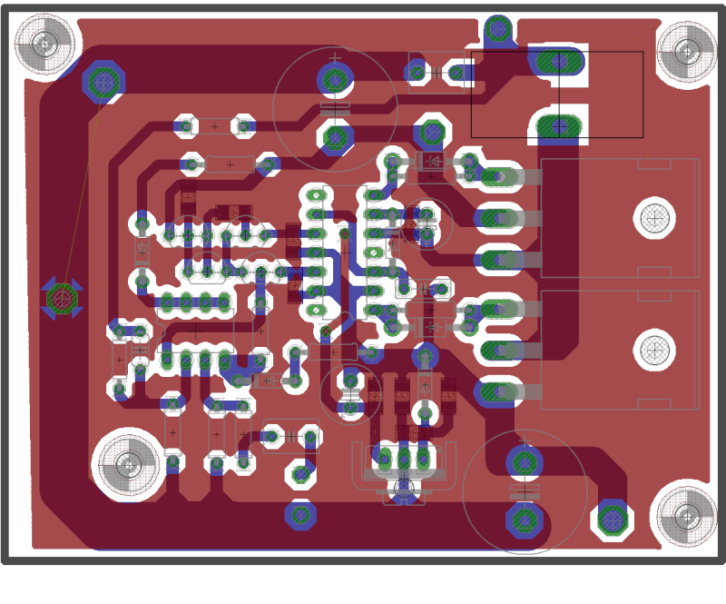
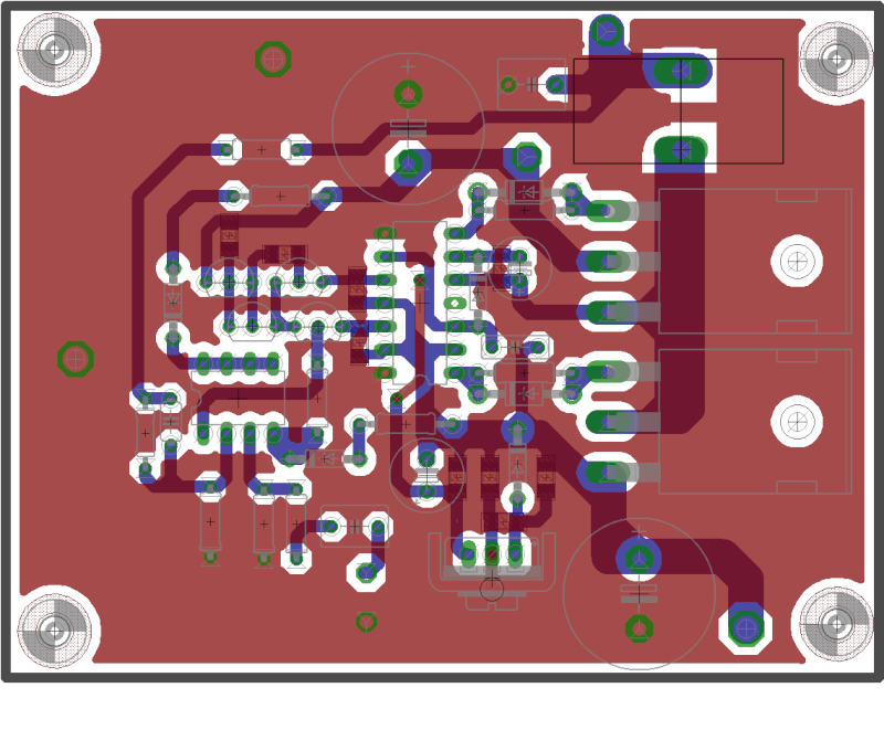
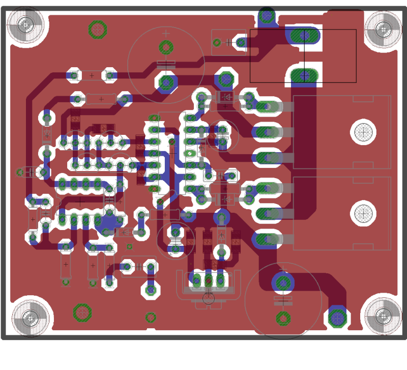
Is good this PCB?
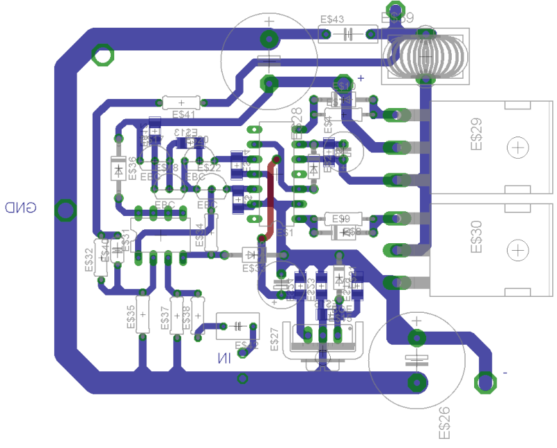
Not very good, but best here so far.
Not very good, but best here so far.
Why not very good? What can you improve? Thanks.
@ akraj
here it is original .pcp file for pcb wizard
Thanks Dzony988. Can i make PCB without any modificaiton? how was your experience of this amp?
This PCB?
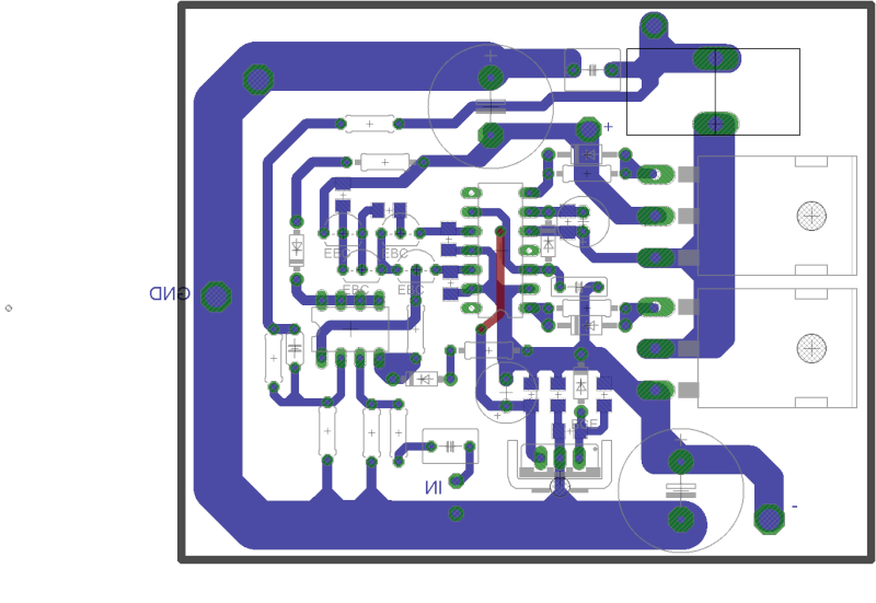
The width of the tracks is not that much a problem.
The biggest problem is that each cycle there are currents flowing through both supplies and ground. Body diode conduction at hard switching is one of them.
The way it flows in your PCB is through GND connection which goes round the whole board with all the sesnitive circuits inside the loop, also it includes input audio ground.
Is that really that hard to accept continous unbroken ground plane?
I could design a good PCB for this design if the people are interested, but I would have my terms...
darkfenriz... the problem is that most of the users on this forum that can design PCBs are experienced in standard PCB design not RF PCB design.
People try to understand the following:
If you use unshielded cables for audio amp input you will have lots of unwanted noise at the output.
The same principle applies to class d amps. they have to be as shielded as possible in order to work properly. other important thing is to use traces as short as possible especially power and signal traces and also you have to avoid loops as much as possible.
regards,
savu
Here are my scope pictures (and the test setup)
An externally hosted image should be here but it was not working when we last tested it.
An externally hosted image should be here but it was not working when we last tested it.
An externally hosted image should be here but it was not working when we last tested it.
- Home
- Amplifiers
- Class D
- UCD 25 watts to 1200 watts using 2 mosfets