original article link:
http://aycu32.webshots.com/image/27431/2004932717725309696_rs.jpg
There are some comments from Amplifier Guru Aka Greg regarding Ian's schematic,
http://www.diyaudio.com/forums/showthread/t-65286-p-3.html
what do you think about these comments?
http://aycu32.webshots.com/image/27431/2004932717725309696_rs.jpg
There are some comments from Amplifier Guru Aka Greg regarding Ian's schematic,
http://www.diyaudio.com/forums/showthread/t-65286-p-3.html
what do you think about these comments?
Attachments
Re: more thoughts on non switching output
It is full amplifier. Buffer (follower) example is, say, here: http://gaydenko.com/audio/ab-dynamic/cdcd01.png
All ab-dynamic-related links were changed - see http://www.diyaudio.com/forums/showthread.php?postid=1704560#post1704560
atiq19 said:
It is full amplifier. Buffer (follower) example is, say, here: http://gaydenko.com/audio/ab-dynamic/cdcd01.png
All ab-dynamic-related links were changed - see http://www.diyaudio.com/forums/showthread.php?postid=1704560#post1704560
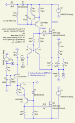
On Hegglun's 50W amplifier, I guess it is not non-switching on closer inspection. I assumed the Source sense resistors were for modulating bias, but I see they are for linearization of the Mosfets.
However, the design may be mod-able to non-switching by replacing R13 and R14 with current sources (maybe with a higher value resistor in parallel) This would produce a logarithmic variation in bias current from the variation of output voltage to rails (due to the small voltage variation across the D1,D2 diodes versus the D3,D4 diodes). As Greg suggested in his comments, the diodes likely should be replaced by matched transistors in diode configurations for better thermal tracking. One could also just try some low resistance across the D3,D4 diodes instead of current sources for R13,R14 to get non-switching.
The high impedance drive of the Mosfet gates may not be a big factor for a non-switching design. Nothing to turn off after all, and Hegglun seems to have gotten high speed besides.
For a buffer, the input would be at the D1, D2 junction, so no Op. Amp. involved.
-----------------
On the ab-dynamic and Renardson class B designs, I would have to see some simulation results or at least an explanation of how they perform. I see components there that obviously modify the bias, but they look to me as if they are doing a linear bias variation, which would just result in class A current ramping. Usually one needs some sort of non-linear control. I'm probably missing some subtle details there.
Don
As for AB-dynamic, there is non-linear control: drain current depends on gate voltage in non-linear manner, doesn't it?smoking-amp said:On the ab-dynamic and Renardson class B designs, I would have to see some simulation results or at least an explanation of how they perform. I see components there that obviously modify the bias, but they look to me as if they are doing a linear bias variation, which would just result in class A current ramping. Usually one needs some sort of non-linear control. I'm probably missing some subtle details there.
Don
atiq19 said:thanks for clarifying, Anli. I see simulations and transfer functions are available on your site. However, a brief description of your circuit would be much appreciated.
It's here: http://www.diyaudio.com/forums/showthread.php?s=&threadid=99313
BTW, during these 1.5 years (after completing AB-dynamic) I have not any thoughts to invent yet another amplifier - just am listening to music
")
atiq19 said:
I disapprove. He's got the MOSFET finals connected as grounded source amps, which is going to mean a hellacious Ci. Secondly, this complimentary SEPP pull up/pull down circuit works much better with BJTs. An NPN/PNP complimentary pair is a good deal more complimentary than any N-Channel/P-Channel "complimentary" pair. If you're going to be using MOSFETs, better to use one kind or the other, but not both. Also, keep 'em out of Class AB. These things have the absolute worst crossover behaviour of any active device. Adapting a topology originally intended to work with BJTs isn't a good idea, but they do it all the time. After all, no OPT is cheaper than the cheapest OPT.
There are some comments from Amplifier Guru Aka Greg regarding Ian's schematic,
http://www.diyaudio.com/forums/showthread/t-65286-p-3.html
what do you think about these comments?
Not much. Before he got himself banninated, Greg was a shameless self promoter, and had (and still does) a vested interest in that "Simple Killer Amp" for which he made a whole bunch of grandiose claims.
Miles,
I see where you coming from. I personally believe, MOSFET amps biasing in class AB is not a good idea. In this regard, I would probably go with Mr Pass's philosophy of high Class A biasing like Aleph series.
Nonetheless, I would go with BJT topology first before trying out complementary MOSFET scheme. In this regard, I believe Anli's design excels in quasi N-channel output, dynamic biasing, avoidance of distortion that arises from solid state heat transfer phenonmenon etc.
However, I had patent 05057790 in my mind before starting this thread. I found the claim using complete non staurating active devices as opposed to partial feedback non switching scheme (which is achieved using switching diodes) quite intriguing. I remember when Mr Pass said his non switching and non MD patent does not achieve neither of them in absolute term, then I thought lets talk about this with our forum friends and gain some insight.I am not quite sure why there is little information about non-switching class AB amps available.
Anyway,
My simulation shows low THD w/out gnfb in Ernest Landi BJT output. How do you probe into transfer function using multisim? I need to see how ouput transistors are avoiding complete cutoff.
later..

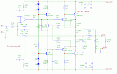
"looks like patent 5057790 is prone to odd order harmonics. about 7 to 15 db more in a range. what could be the solution?"
Q5 and Q6 look awfully starved for operating voltage, try putting some diodes in series with the Q3 and Q4 emitters. Ohh, I see they did that already on figure 5 with V10&U60, well put even more diodes in. If you put enough diodes in (use LEDs), you could even try some Mosfets for Q5,Q6.
A symmetrical sliding bias scheme is always going to produce odd harmonics, you just want to get something smooth enough to minimize them. Maybe Anli's quasi scheme is better at avoiding odd harmonics?
----------------------------------
"I disapprove ......"
Well I agree with some of Miles comments here on Mosfets, BUT the Hegglun circuit design IS specifically oriented toward linearizing them via the current sensing drivers. It doesn't much care what the final outputs are made from (could try tubes even), it just makes the current out proportional to the signal in. The drivers should isolate the Mosfet Cin from the input at D1,D2 too, although I would still use low capacitance, late model Mosfets. (Fairchild comes to mind.)
-------------------------------------
"A picture speaks of thousand words! Would it be possible to post a schematic for Hegglun non switching mods you proposed? I will try to simulate it with multisim."
The basic idea here is to get the D1,D2 voltage drops to mistrack versus the D3,D4 voltage drops. (notice RV1,RV2 set idle bias)
I think some playing around on the simulator is going to be required to find something working properly for sliding or non-switching bias here. As presently configured with resistors R7,R8,R13,R14 to the rails, the current thru those diodes varies as the output voltage swings, but both sides track and cancel. So we want to get one side mistracking some in the right manner. We need to increase the bias as the output swings toward either rail.
Some ideas:
1) double up the diodes on the D3,D4 side and compensate (for idle condition) with low value resistors in series with D1 and D2.
2) put CCSs in place of R13,R14 to keep constant drops on D3,D4.
These 1) & 2) aproaches will only work for a fixed load impedance, since we are only controlling bias currents via output voltage swing. The better schemes control via the output currents. So:
3) put some low Ohm sense resistors in series with the Mosfet drains, and then couple some high value resistors from the drains to the respective D3,D4 diodes.
4) seems waistfull to have to use two sense resistors for each Mosfet, so we need to try using the existing R17,R18. Tempting to try diodes in place of R17,R18 but that gives the wrong variation I think. So I would try a series diode in the T4 and T8 emitters and a compensating resistor in series with the T3 and T7 emitters. Ironically, we are making the outputs non-linear using the linearizer driver! If the diodes have too much effect, then put resistors in parallel with them (and compensate the comp. resistors too). Could also try Mosfet "diodes" in place of the T4,T8 emitter diodes. Numbing tweaking of resistors may be required here to get this working right.
Solving #4 obviously is the preferred approach.
---------------------------------------
"As for AB-dynamic, there is non-linear control: drain current depends on gate voltage in non-linear manner, doesn't it?"
Yes indeed, my thoughts were a little locked onto bipolar sliding bias schemes where tiny mis-tracking junction voltages are usually used.
Since power tubes also have an approx. square law response, it might be interesting to make a non-switching output tube amp too. See Broskie's link below:
--------------------------------------
http://www.tubecad.com/2006/12/blog0091.htm
Don
Oops. On the Landi patent fix suggestion I made above, obviously one cannot endlessly put more diodes in the Q3,Q4 emitters without either frying the outputs or increasing the output emitter resistors. I see figure 5 of Landi uses 2 Ohm emitter resistors after adding one set of diodes (V10,U60). Looks like the extra diodes gets impractical fast.
Well, if you can't fix it, cheat:
Separate the Q5 and Q6 emitters and use two separate R7 resistors to cross connect them to the emitters of Q1 and Q2. That way you get the voltage drop across two emitter resistors for operating Q5,Q6.
edit:
On second thought, thats not going to work, since the voltage variation across the two output emitter resistors is complementary. Looks like one has to use some ugly current sources from the rails down to separated Q5,Q6 emitters (or maybe to their collectors with additional diodes to the Q3,Q4 bases) to get more voltage. How about using vertical Mosfets for the outputs instead. I wonder if this patent is actually used in any product?
Don
There is the Linear Technology LT1166 chip that is supposed to do non-switching crossover control for vertical Mosfets. But comments I've heard were that it didn't do that well on distortion, and I think there was a thread somewhere on the SS forum about it, that concluded that it had a design flaw in it. If Linear Tech. would fix their chip, this crossover stuff would be trivial. But maybe some ideas can be gleaned from its design for a discrete version.
Don
Don
Now I realise why sliding bias didn't get popularity! Complications for nothing??
Here is infamous LT1166 (discrete) cracked by SY08. If you scan through Error correction thread, you would see that this chip doesn't live up to the claim either.
I need to find some directions in practical term.
Many thanks Don.
Here is infamous LT1166 (discrete) cracked by SY08. If you scan through Error correction thread, you would see that this chip doesn't live up to the claim either.
I need to find some directions in practical term.
Many thanks Don.
Attachments
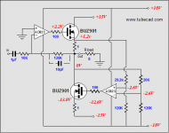
The tubecad design looks like it is class A. Can you give a link?
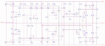
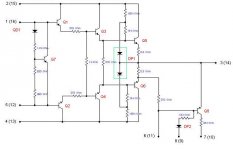
The Technics chip is a mystery to me. Obviously Q8, DP1 and DP2 are extra parts from normal. But I don't see what they are doing. Some external stuff must be going on at the pins 6(11),8(9) & 7(10).
Take a look at patent # 4,570,129 by Milberger for a simple non-switching bias scheme. It should be readily adaptable for a complementary source follower setup. But its the Mosfet turn-on voltages that are providing the operating headroom for the bipolar feedbacks. Mosfet outputs would rescue the Landi design too.
If you look up the patents referenced by Landi and then use the Patent Office link to find referenced patents and refering patents, for each of those (including from Landi), there are a number of other sliding bias schemes around which don't directly show up by obvious searches. Some of these could be useable. No way to know how well they work though except maybe by simulation. But the schemes generally are operating the bipolars with very low voltages which don't simulate accurately.
Don
- Status
- This old topic is closed. If you want to reopen this topic, contact a moderator using the "Report Post" button.
- Home
- Amplifiers
- Tubes / Valves
- Tube Amp Compensation Q