I only show 'Loop Gain' cos several people are pontificating about how this is the answer to Life, the Universe & Everything.
You seem to have missed the point.
There are several loops so there are several Loop Gains, or as a reader of Bode would prefer, Return Ratios.
The outer-most loop is all you have shown. This is not a reliable indicator to stability in a multi-loop amp.
This misconception caused interminable confused debate in the TMC/TPC thread before it was finally understood and a reasonable consensus reached.
Some of the rest of your post is also a result of this same misconception so I won't answer it point by point if I can avoid it.
Please don't start that debate again!
Read especially JCX's posts in the TPC/TMC debate and then Bode plot the other loops in your OIC and TMC amps.
In your amps the output transistors are about 20 times slower than the other transistors.
Yet you have the same loop ULGF about them in your OIC amp as the loop around just the IS in TMC.
That is not reasonable.
Best wishes
David
Last edited:
I did name one when its designer extolled its virtues on this forum. The 'gentleman' (?!?)immediately disowned it and I was banned
Were you posting under the kgrlee name at the time? I might dig it up for my own sordid amusement.
In Jurassic times, I amended Cherry's 1982 matrix analysis to take these out. (I cud reed en rite in dem daz.)
And presumably found the arrangement satisfactorily stable, hence your ongoing recommendation?
Plis dun mek fun orf mi. Us pipul hu kunt reed en rite r sensitive bout it.
Wozint maykin funn ov yue. Woz maykin funn ov thi 4um. Ime a qweanslander tu. Bye thi waye, oi thinck yue speld sencitif rong. Uz gangg gut tue stik tugether.
Going back to PCC, do you think the bootstrap is important? My speculation is that it relates the impedance of the VAS current source load to the slow output transistors in a way that helps, hinders or is neutral. (I'd hate to be wrong about that last part but you gotta go out on a limb sometimes.)
[deleted: six pages of 'first rate, innovative' writing (according to Douglas Self), dating from circa July 1997. It's too big for the 4um to handle. Send me a private message with your email address.]
Dave, you are correct.There are several loops so there are several Loop Gains, or as a reader of Bode would prefer, Return Ratios.
The outer-most loop is all you have shown. This is not a reliable indicator to stability in a multi-loop amp. This misconception caused interminable confused debate in the TMC/TPC thread before it was finally understood and a reasonable consensus reached. ... etc
But I have never said the outer loop response is a reliable indicator bla bla. In fact I say this and the other loop responses are probably the least useful to assess stability. Please read my sh*t a bit more carefully.
But the point I made was that if you really want a 'linear' measure of stability, just close the loop. If ANY of the inner loops peak or have nasty 'margins', this will appear in the closed loop response if they are important.[*]
Of course this will not give you any idea of non-linear 'parasitics' but none of the 'linear' stability measures do this either.
The old pedantic measures ARE useful if you are trying to improve stability though.
[*]One which doesn't appear cos its unimportant is the mid peak with TPC.
__________________
.. and more importantly, in 'real life' too. But I would NEVER have 20cm between the PCB and the driver bases like CherrySteve49 said:(concerning removing Cherry's Ccb on the drivers).... And presumably found the arrangement satisfactorily stable, hence your ongoing recommendation?
And if you need dem Ccb, they are useless on the PCB or on the VAS. They have to be AT the drivers. So I HAVE tried them.
If you mean Cherry's use of a bootstrapped resistor instead of a CCS on the VAS, most people find that the CCS gives less 20kHz distortion. It was 20 yrs before the 90's activity that I built an amp with a bootstrap VAS load.Going back to PCC, do you think the bootstrap is important?
So I can't answer your question cos I haven't tried it since I were a lad.
______________
BTW, I try to post ONLY stuff that has some resemblance to what I've seen in 'real life'.
I don't expect to see 1ppm THD @ 20kHz with even the best layout, decoupling & earthing. But I do expect a good 'pure Cherry' to beat a good TMC if equal care is taken with both .. cos I've done something similar in 'real life'.
I'm offering these 3 examples for people to shoot down or improve .. at least in SPICE world. And the tools & methods I use to assess them.
I'm perfectly aware that my previous 'real life' experience with 'pure Cherry' might bias my efforts with lesser approaches. So I'm hoping the TPC/TMC gurus might improve my crude TPC/TMC models.
Rules: You may change or move/change any and all resistors/capacitors but no more or better active devices except diodes. You can throw active devices out and move them.
Are my examples too complicated and obfuscating to use? Comments / questions?
______________
Conversely, if you have a .ASC with 'accurate' device models which you believe is a good representation of a 'real' amp with TPC / TMC, I would like to try and improve it using 'pure Cherry'.
But not too complex please. I don't think 'pure Cherry' is good for 'triples + supa dupa VAS' ... but why do you need them if you already have 1ppm THD @ 20kHz.
Last edited:
If I do understand David right, then he is concerned about the robustness of the circuit in reality. As you pointed out elsewhere, Spice simulation only gives us estimates about reality.But the point I made was that if you really want a 'linear' measure of stability, just close the loop. If ANY of the inner loops peak or have nasty 'margins', this will appear in the closed loop response if they are important.
[*]
Of course this will not give you any idea of non-linear 'parasitics' but none of the 'linear' stability measures do this either.
The old pedantic measures ARE useful if you are trying to improve stability though.
[*]One which doesn't appear cos its unimportant is the mid peak with TPC.
So, it is good practice to evaluate as many as possible savety margins, e.g. stability margins in all important loops or SOA margins, just as another example.
In circuits here in the forum, one often sees a quite sharp 'knee' in the global loop reponse, perhaps stemming from a stability issue in the (darlington) VAS. If you distinguish between important and unimportant problems, would this be an important one?
(Your global loop response for Miller compensation including OPS, post #4, does show such a knee at about 10MHz.)
Best regards,
Matthias
PS to post #46.
In the "pure Cherry" circuit from post #4, you seem to compensate an OPS pole using C9. The value seems to depend on the OPS transistor type.
One can dimension C9 just by looking on the loop response of the global loop (or even on the transient response ...). IMHO, directly probing the Miller loop (independently and together with the additional gain when closing the GNFB loop) really helps in understanding the circuit behaviour and in detecting possible problems.
With the rather low stability margins, it further would be useful to probe the loops at different OPS output currents and voltages. I definitely second godfrey.
Best regards,
Matthias
Last edited:
Well my little grouse in this case is that David may not have bothered to read all my stuff.If I do understand David right, then he is concerned about the robustness of the circuit in reality. As you pointed out elsewhere, Spice simulation only gives us estimates about reality.
So, it is good practice to evaluate as many as possible savety margins, e.g. stability margins in all important loops or SOA margins, just as another example.
You are right about these extra loops but IMHO & E, the Closed Loop response is an accurate linear indication of what's happening in ALL the inner loops too. The important variation is to look at it with various loads & some changes in devices.
BTW, I'm only doing in LTspice what I used to do in 'real life'.
In fact I design for just this behaviour.In circuits here in the forum, one often sees a quite sharp 'knee' in the global loop reponse, perhaps stemming from a stability issue in the (darlington) VAS. If you distinguish between important and unimportant problems, would this be an important one?
(Your global loop response for Miller compensation including OPS, post #4, does show such a knee at about 10MHz.)
Bode proposed his 'ideal behaviour' with a slope of 9dB/8ve and PM=45.
A good approximation to this which I've used successfully in my 'real life' past, is to have 12dB/8ve up to your 'unity gain' freq and 6dB/8ve above that. This is of course how TPC should be done.
I didn't do it properly on my TPC example
Mea maxima culpa. But that's how I used to do TPC type compensation.Alternatively, you can have 6dB/8ve up to unity gain and 12dB/8ve above and this is what's in my 'pure Cherry' example. (Better if this happens above unity gain cos better margins bla bla) Usually easier cos above those frequencies, there's loadsa evil poles. The tweaking cancels ju.uust those which may affect this nice behaviour on the worst possible loads.
Yes. As I said, this is the sort of thing you need to check and do in real life if you change devices in productionIn the "pure Cherry" circuit from post #4, you seem to compensate an OPS pole using C9. The value seems to depend on the OPS transistor type.
Yes. This is what I use Loop Gain plots for ... tweaking stuff better. You do it with different loads bla bla too.One can dimension C9 just by looking on the loop response of the global loop (or even on the transient response ...). IMHO, directly probing the Miller loop (independently and together with the additional gain when closing the GNFB loop) really helps in understanding the circuit behaviour and in detecting possible problems.
Can you suggest where to put a Tian probe to look at the 'pure Cherry' loop?
Michael K showed something in Bob Cordell's thread but I don't think its in the right place to really look at the inner loop.
I think the Closed Loop response is more revealing but I'm a SPICE newby and am open to suggestions.
.TRANS with loadsa loads & different devices is definitely better cos it models output current parameter changes if you want a Yah/Nay stability answer.
The stability margins for the 'pure Cherry' example exceed both Bode's & Cordell's recommendations. My main worry (which is on my list in post #4) is this is happening at 3.5MHz.With the rather low stability margins, it further would be useful to probe the loops at different OPS output currents and voltages. I definitely second godfrey.
Godfrey's method is interesting. But as I said earlier, LTspice actually DOES simulate the 'higher & different output current behaviour'. Some of the versions along the way did have the 'small parasitics on part of the waveform' on certain loads and ... LTspice simulated the 'cures' I used in 'real life'.
I'm really impressed by this.
Perhaps someone would like to show that my 3 examples have inadequate behaviour on these or other tests?
Dunno how my stuff gets accused of needing Godfrey's test just cos I said Golden Pinnae stuff often misbehaves.
My stuff isn't Golden Pinnae so dun misbehave. Thanks for your comments Matze.
Last edited:
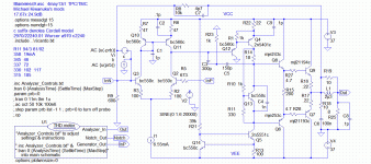
Neither of these compensation circuits have been optimised so I invite the various champions to offer improvements for both configurations on what I think is near a ‘real life’ device.
-lose JFET cascodes and C1, C2
-reduce R7, R6 to 47R
-use independent amplified negative feedback current sources for input stage and second stage.
-reduce R23 to 1K
-increase C3 to 300p
-increase C5 to 150p
-lose C9 and R26
-increase input stage degeneration to 100R each.
Thanks for these suggestions Michael. Are they for the TPC or TMC?-lose JFET cascodes and C1, C2
-reduce R7, R6 to 47R
-use independent amplified negative feedback current sources for input stage and second stage.
-reduce R23 to 1K
-increase C3 to 300p
-increase C5 to 150p
-lose C9 and R26
-increase input stage degeneration to 100R each.
I'm not sure, with all the discussion whether you have a preference for TPC or TMC or if they give the same performance.
Shall I take the collecter of the VAS EF Q12 to ground or can I leave it on the base of Q14 which is part of the amplified NFB current source for the VAS?
Last edited:
Shall I take the collecter of the VAS EF Q12 to ground or can I leave it on the base of Q14 ....
Ground it.
Well my little grouse in this case is that David may not have bothered to read all my stuff.
I do read all your tech. stuff, sorry if I caused a
. I tend to skip the misspelled stuff because it is a bit tedious to my taste. Bode proposed his 'ideal behaviour' with a slope of 9dB/8ve and PM=45.
Bode's actual recommendation was much more complex and subtle than this.
Not even a rational function.
Normally Bob Cordell is clever in his simplification of complicated subjects, but I think he over simplifies this one.
Can you suggest where to put a Tian probe to look at the 'pure Cherry' loop?
On the line between the junction of the output transistor emitter resistors and where the compensation capacitor splits off (C3 in post #4) will show the total feedback around the OPS, which is what matters I think.
The line above C3 doesn't evaluate any actual Return Ratio as far as I can see.
I plan to unzip your examples and put all the models in the correct spots to run this.
But if you can run this before me then I would be interested to see your results.
Best wishes
David
Last edited:
Me, too. And all this for free with a nice interface.... But as I said earlier, LTspice actually DOES simulate the 'higher & different output current behaviour'. Some of the versions along the way did have the 'small parasitics on part of the waveform' on certain loads and ... LTspice simulated the 'cures' I used in 'real life'.
I'm really impressed by this.
Spice has done the evaluation with different OPS output currents and voltages in the transient simulation, and no problems became evident. This does mean, that *exactly* this circuit behaves that way. But it does not give you an estimate how robust the circuit will be against e.g. device parameter variations or parasitic elements in a real piece of hardware.
(Are the circuits exactly the same you tried out in 'real life', i.e. with same transistor types and so on?)
Best regards,
Matthias
Also useful is C9 across the VAS emitter resistor.
The possibility of a zero from C9 looks useful to me too.
However, Cherry's 1982 JAES paper showed that the amplifier is remarkably insensitive to variation of the impedance of that emitter resistor.
So does it make much difference to lower the impedance with a bypass capacitor?
In the "pure Cherry" circuit from post #4, you seem to compensate an OPS pole using C9. The value seems to depend on the OPS transistor type.
One can dimension C9 just by looking on the loop response of the global loop (or even on the transient response ...). IMHO, directly probing the Miller loop (independently and together with the additional gain when closing the GNFB loop) really helps in understanding the circuit behaviour and in detecting possible problems.
Hi Matthias
Same question about C9 to you!
And concur about importance to probe the Miller loop in OIC.
Your thread on Nested Miller Compensation is an excellent example of a deceptively innocent outer loop that concealed problems.
How you came to understand and solve this is very educational.
I recommend it to kgrlee.
Best wishes
David
Damir, will you try my .ASC files and suggests values for better performance from the TPC & TMC version? I've tried to make it as easy as possible for people to do this. I don't care what 'margins' etc are .. just what stability the final amp has.
As I've said ad nauseum, my stability criteria isn't a 'linear' measure like Phase/Gain Margin/Nyquist .. but what happens on different loads on both Close Loop .ASC and .TRANS in SPICE world .. and the same in the 'real world'.
This is what the outside 'real world' sees.
]
Here are some simulations with your amp, TPC vs. TMC. I changed a bit your shematic to simplify it a bit and removed C7 as Cordell does't like it. It's not that I want to increase your nausea, I put here Phase and Gain margin at the same level, showed Nyquist for CLG, and simulated distortion. In my simulation TMC wins by small margin with lower THD20k.
Regarding real world load simulation you have not showed what it is.
One question: I could not get thd_percent graph, with notch_out it was OK.
BR Damir
Attachments
Michael Kiwanuka's version
Gentlemen, I simulated the TPC & TMC version with Michael's recommended mods. I've used a perfect CCS, I1 for the LTP cos in this sim, with perfect supplies, it makes little difference.
Assuming a 'independent amplified negative feedback current source' takes 2 devices, this gives him a spare active device in hand cos he removed the input cascodes. I've left the VAS load 'fully' simulated cos it has substantial effect on performance so needs to be accurate.
Please note several caps have a value of .1p This is much less than the stray cap across a thru' hole resistor so is my crude way of removing caps which I may want again later.
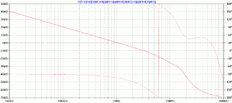
His versions have better 'stability margins' but also much higher distortion. I've included the evil Loop Gain plots cos I need some sort of 'stability' measure to fudge the 'pure Cherry' version to compete on equal terms. I maintain and accept that simple 'linear' stability margins tell you little bla bla ... and prefer to judge stability on behaviour with different loads with .TRANS bla bla ... both in SPICE & 'real' worlds bla bla
First his TPC version.
Gentlemen, I simulated the TPC & TMC version with Michael's recommended mods. I've used a perfect CCS, I1 for the LTP cos in this sim, with perfect supplies, it makes little difference.
Assuming a 'independent amplified negative feedback current source' takes 2 devices, this gives him a spare active device in hand cos he removed the input cascodes. I've left the VAS load 'fully' simulated cos it has substantial effect on performance so needs to be accurate.
Please note several caps have a value of .1p This is much less than the stray cap across a thru' hole resistor so is my crude way of removing caps which I may want again later.
His versions have better 'stability margins' but also much higher distortion. I've included the evil Loop Gain plots cos I need some sort of 'stability' measure to fudge the 'pure Cherry' version to compete on equal terms. I maintain and accept that simple 'linear' stability margins tell you little bla bla ... and prefer to judge stability on behaviour with different loads with .TRANS bla bla ... both in SPICE & 'real' worlds bla bla
First his TPC version.
Attachments
Last edited:
and the winner, "pure Cherry"!
But yus guys will have realised, my evil mission is to promote 'pure Cherry' over evil TMC and even TPC.
Michael's versions have greater 'stability margins' than those in posts #1, 2 & 4 which use Bode's & Cordell's recommendations.
For a fairer comparison, I've reduced the Loop Gain of the 'pure Cherry' from post #4, by 10dB. This is done by making C1/3, the 'compensation' caps 150p ... and C9, the cap across the VAS emitter resistor 470p.
You'll note it still has nearly 20dB THD advantage over his TPC & TMC versions, even with its loop gain hobbled like this.
Attachments
Gentlemen, I shan't be able to post more until sometime next week. But please carry on this most useful discussion. In the meantime ..
David, in his 82' paper, Cherry does 2 analysis. One at LF, looks at THD. It is this that shows the 'insensitivity' of the VAS emitter resistor.
The other analysis is of HF stability. There, the VAS emitter resistor is very powerful. In da dim & distant past, I extended his matrix to stuff connected to the VAS emitter resistor and removed some of his other evil caps.
Damir, the instructions for using the THD meter are in 'Analyzer_Controls.txt'. I made THD.plt to simplify the last step to show all 10 harmonics. The models are set to do the THD plots directly. They take a long time to do on my PC ... 2 or 3 cups of coffee.
The 20k residual plots are V(out)/283000 (for a 0.01% reference fundamental) and V(notch)/28.3 to give the residual. You do these on the RAW display. The 20kHz residuals are from 0.5ms to 0.6ms
More next week.
But yus guys will have realised, my evil mission is to promote 'pure Cherry' over evil TMC and even TPC.
kgrlee,
As I've pointed out many times before, Cherry's output-inclusive compensation is not stable because the second stage continues generating gain long after the output stage poles have taken effect.
What is required is shunt capacitive compensation at the second stage's collector to roll off its gain to below unity before the output stage poles come into effect.
But you should note that shunt capacitance at the second stage's output compromises its linearity.
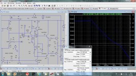
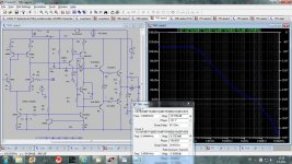
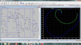
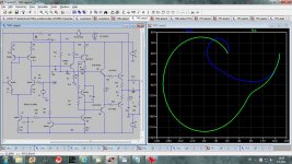
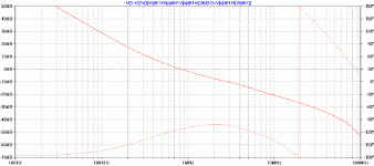
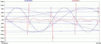
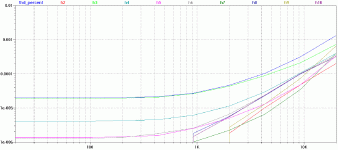
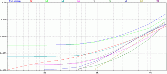
Below is a minor loop gain sim of an amplifier with OIC with (blue trace) and without (green trace) shunt compensation (1nF) at the second stage's output.
Note that although the blue trace (with shunt compensation) is stable in this simulation, its unity loop gain frequency is roughly 9MHz, which, I suspect, would still lead to instability in a real amplifier whose output stage dominant poles are likely to reside at somewhat lower frequencies if power BJTs rather than MOSFETs are used.
Attachments
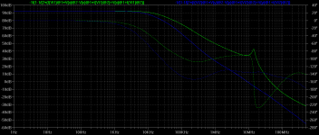
Below is a minor loop gain sim of an amplifier with OIC with (blue trace) and without (green trace) shunt compensation (1nF) at the second stage's output.
Mike, your two-transistor VAS/TIS and triple output is outside what kgrlee is proposing (and what Cherry analysed); see post #4 in this thread. Also, you don't have the VAS/TIS emitter resistor and kgrlee's parallel capacitor. Does addressing these issues change the outcome?
Potentially the bootstrap VAS/TIS load and the load stabilising network should be added also (post #41), though I don't know whether these have any significant influence.
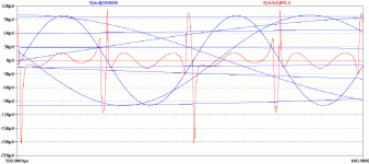
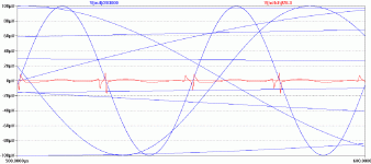
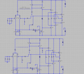
On the method of simulating the inner loop gain, I've seen others disable the global loop with a massive inductance in series with the global feedback resistor. Is that what you have also? In the bottom schematic, the feedback component looks like an inductor, but in the top circuit it looks like a resistor. Maybe just the grid points blurring the picture.
kgrlee,
Below is a minor loop gain sim of an amplifier with OIC with (blue trace) and without (green trace) shunt compensation (1nF) at the second stage's output.
Hi Mike (and kgrlee)
Could you please turn off the grid to reduce the clutter on your circuits?
White background would help a bit too.
Results look very plausible but it's a bit hard to tell!
Best wishes
David
- Status
- This old topic is closed. If you want to reopen this topic, contact a moderator using the "Report Post" button.
- Home
- Amplifiers
- Solid State
- TPC vs TMC vs 'pure Cherry'