Hi Minek, Thanks for asking.
Hi All,
") .
.
BTW none of my circuits are patented, they are all in the public domain and free for all to use.
I have updated Post 1 summary of key posts.
Thanks to all who have already contributed to this thread!
Anyone is welcome to add more to this thread. Please do.
Cheers,
Ian Hegglun
Hi All,
I think that about does itPost 1 "Well, there's the challenge. A wideband non switching Auto Bias amplifier circuit that works, doesn't oscillate and blow up, and is not too complex."
.BTW none of my circuits are patented, they are all in the public domain and free for all to use.
I have updated Post 1 summary of key posts.
Thanks to all who have already contributed to this thread!
Anyone is welcome to add more to this thread. Please do.
Cheers,
Ian Hegglun
Hi Keantoken,
Re: kenpeter lately?: https://www.diyaudio.com/community/threads/any-news-from-kenpeter.374139/
Re: kenpeter lately?: https://www.diyaudio.com/community/threads/any-news-from-kenpeter.374139/
Great project Ian, it's good to see a worthwhile project defined, undertaken and brought to a successful completion. Chapeau!Hi Minek, Thanks for asking.
Hi All,
I think that about does it
BTW none of my circuits are patented, they are all in the public domain and free for all to use.
I have updated Post 1 summary of key posts.
Thanks to all who have already contributed to this thread!
Anyone is welcome to add more to this thread. Please do.
Cheers,
Ian Hegglun
What's next on your list ?
Jan
Hi Jan,
Thanks. IIRC when I started this thread I asked you for options and you suggested AudioXpress since they are "... slowly moving in a more technical direction" here https://www.diyaudio.com/community/...udio-is-over-what-is-next.340324/post-5854495
Another option is develop a discrete 8 pin DIP to supersede the LT1166. Recall this?

BTW this autobias is much faster than the LT1166 since it does not use opamps like the LT1166.
The other feature that makes it superior to the LT1166 is there are no emitter resistors (or source resistors) which gives excellent open-loop linearity in Class-AB with a reasonably low optimum biasing (see measured plot Post 154). Open-loop linearity is good. You don't need additional feedback or gain stages like the standard topology -- which needs lots and lots of feedback because emitter/source resistors are used in the power stage.
My complete autobias current drive amp sounds great with only 6dB of local feedback!
But if you want to drive standard speakers you need to use more feedback -- just to get the output resistance down -- the amount of nfb depends on your loudspeaker impedance vs frequency plot and how particular you are about slight changes in frequency response due to the amps Rout.
BTW2 when I had a set of JV60 speakers, I found 6 ohms amplifier output impedance was acceptable, at least for my ears. You may recall you published this in Linear Audio Vol. 1.
Erratum: Q6 is shown as {Temp2} but should be {Temp1} which is Tamb.
Thanks. IIRC when I started this thread I asked you for options and you suggested AudioXpress since they are "... slowly moving in a more technical direction" here https://www.diyaudio.com/community/...udio-is-over-what-is-next.340324/post-5854495
Another option is develop a discrete 8 pin DIP to supersede the LT1166. Recall this?
The tricky bit is Q1 needs to be mounted on one of the Schottky diodes. I think it can be done by omitting the COM pin. Q1 base then uses 'COM' pin and Q1 emitter then uses 'Vtop' pin. Bias resistor R14 could be a pick and place resistor with machined plugs as part of the discrete 8 pin DIP (or maybe an EEPROM pot so the DIP can be sealed).BTW, I'm still fiddling with auto bias circuits, one the holy grails in audio. If one gets it truly right (without adding any distortion), that would mean a major step forward. Post 3308
BTW this autobias is much faster than the LT1166 since it does not use opamps like the LT1166.
The other feature that makes it superior to the LT1166 is there are no emitter resistors (or source resistors) which gives excellent open-loop linearity in Class-AB with a reasonably low optimum biasing (see measured plot Post 154). Open-loop linearity is good. You don't need additional feedback or gain stages like the standard topology -- which needs lots and lots of feedback because emitter/source resistors are used in the power stage.
My complete autobias current drive amp sounds great with only 6dB of local feedback!
But if you want to drive standard speakers you need to use more feedback -- just to get the output resistance down -- the amount of nfb depends on your loudspeaker impedance vs frequency plot and how particular you are about slight changes in frequency response due to the amps Rout.
BTW2 when I had a set of JV60 speakers, I found 6 ohms amplifier output impedance was acceptable, at least for my ears. You may recall you published this in Linear Audio Vol. 1.
Erratum: Q6 is shown as {Temp2} but should be {Temp1} which is Tamb.
@All,
An interesting variation of the LT1166 autobias variant by ttlhacker
https://www.diyaudio.com/community/...deband-auto-bias-amp-design-and-build.392549/
and I have modified it for higher voltages and reduced the number of stages while still giving good sim performance (not bench tested).

An extra mirror stage is added to sense current in the power transistors emitter resistors and Schottky diodes. The bias current for I1 and I2 is adjusted for 130mA idle current or 10W idle dissipation (nice). The THD is 0.006% at 1kHz 80W just below clip. Compensation is easy with C3 and C4.
A +/-5V auxiliary supply allows low voltage transistors with high voltage power transistor rail voltages. It reduces dissipation in the driver transistors. But one twist with 5V to the driver transistors is clip recovery gives a nasty 1us high current cross-conduction spike in the power transistors until the autobias starts up. This is negated by adding C8+R3 across the power transistor bases after the base stopper resistors, which may be useful in other autobias loops .
The interesting thing with this type of autobias compared to my last design is the Schottky diode temperature change does not much affect the idle current so is free from thermal time delays in both the power transistors and Schottky diodes. In my last design the Schottky diode temperature change, first at start and after full power, is tricky to accurately thermally compensate and there is a time delay.
BTW The attached file contains a voltage follower version that does not need a floating main power supply, but needs a floating +/-5V supply - a 1W DCDC brick converter can be used for this which is not expensive. A high voltage VAS stage or a HV opamp is used for voltage gain.
An interesting variation of the LT1166 autobias variant by ttlhacker
https://www.diyaudio.com/community/...deband-auto-bias-amp-design-and-build.392549/
and I have modified it for higher voltages and reduced the number of stages while still giving good sim performance (not bench tested).
An extra mirror stage is added to sense current in the power transistors emitter resistors and Schottky diodes. The bias current for I1 and I2 is adjusted for 130mA idle current or 10W idle dissipation (nice). The THD is 0.006% at 1kHz 80W just below clip. Compensation is easy with C3 and C4.
A +/-5V auxiliary supply allows low voltage transistors with high voltage power transistor rail voltages. It reduces dissipation in the driver transistors
. But one twist with 5V to the driver transistors is clip recovery gives a nasty 1us high current cross-conduction spike in the power transistors until the autobias starts up. This is negated by adding C8+R3 across the power transistor bases after the base stopper resistors, which may be useful in other autobias loops .The interesting thing with this type of autobias compared to my last design is the Schottky diode temperature change does not much affect the idle current so is free from thermal time delays in both the power transistors and Schottky diodes. In my last design the Schottky diode temperature change, first at start and after full power, is tricky to accurately thermally compensate and there is a time delay.
BTW The attached file contains a voltage follower version that does not need a floating main power supply, but needs a floating +/-5V supply - a 1W DCDC brick converter can be used for this which is not expensive. A high voltage VAS stage or a HV opamp is used for voltage gain.
Attachments
An interesting variation of the LT1166 autobias variant by ttlhacker
https://www.diyaudio.com/community/...deband-auto-bias-amp-design-and-build.392549/
and I have modified it for higher voltages and reduced the number of stages while still giving good sim performance (not bench tested).
Super nice, thumbs up!
Some minor notes:
The two outputs of the OTA could be connected directly to the compensation caps, skipping the series resistors. This will improve the gain margin of the OTA feedback loop dramatically, while keeping the damping for the autobias feedback loop. (You'd have to flip the order of the cap and resistor - cap to ground, resistor above, OTA connecting to it in the middle)
I5/I6 have to be equal to the minimum current that's expected to flow through Q4/Q23. This improves the current sensing accuracy at lower bias currents (where it matters the most). It seems to be correct in the design you posted (there should always be more than 50mV across the current sense resistors, which means there's at least 1mA flowing through Q4 and Q23).
I'm slowly building the original (more complicated) version of this design over in the linked thread. I really hope it'll work!
H Ian,... The interesting thing with this type of autobias compared to my last design is the Schottky diode temperature change does not much affect the idle current so is free from thermal time delays in both the power transistors and Schottky diodes. ...
Really over my head. Could you elaborate a bit more on the reasons of how ΔVF of the Schottky diode due to ΔT (ambient and self dissipation) does not effect idle current as much as the autobias action that depends on ΔVF due to ΔIF.
Do you see any disadvantage in directly detecting VBE of output transistor instead of using a Schottky for this scheme?
I intend to use the previous scheme on lower power 10-25W amps, different need than yours. The plan is to have as uniform power dissipation as practical from idle to max power output to reach a somewhat steady state thermal equilibrium. However a compensation is absolutely required to stabilize IQ against ambient ΔT, an NTC as you suggested would be simple enough.... In my last design the Schottky diode temperature change, first at start and after full power, is tricky to accurately thermally compensate and there is a time delay....
Hi indra1,

Reducing I1,I2 to 3mA can reduces current in the Schottky's further to 3mA and 90mA idle current.
Alternatively, using fast power diodes instead of Schottky's makes the diode idle current almost disappear, then there's virtually no temperature sensitivity to diode temperature. Diode dissipation is higher than Schottky's at high output powers - but that's probably not an issue in typical audio amps since the average power levels are quite low (even with an occasional clip). Some bench tests are needed to quantify these factors.
In the ttlhacker autobias the Schottky diodes are only slightly conducting at idle - plot below. Most of the idle current passes through emitter resistors R5,R8 and not the Schottky's.Could you elaborate a bit more on the reasons of how ΔVF of the Schottky diode due to ΔT (ambient and self dissipation) does not effect idle current as much as the autobias action that depends on ΔVF due to ΔIF.
Reducing I1,I2 to 3mA can reduces current in the Schottky's further to 3mA and 90mA idle current.
Alternatively, using fast power diodes instead of Schottky's makes the diode idle current almost disappear, then there's virtually no temperature sensitivity to diode temperature. Diode dissipation is higher than Schottky's at high output powers - but that's probably not an issue in typical audio amps since the average power levels are quite low (even with an occasional clip). Some bench tests are needed to quantify these factors.
Yes. I prefer autobias arrangements that can interchange bipolar power transistors with MOSFET's without any change to the circuit; usually only a small re-tweak of the idle current. I confirmed that I could change from BJT's to MOSFETs in my previous autobias design in bench tests, without any resistor value changes apart from a re-trim of the idle pot.Do you see any disadvantage in directly detecting VBE of output transistor instead of using a Schottky for this scheme?
One thing that's nice about the diode-clamped current sense resistors is that the dissipation in the diodes rises linearly with output current while the power delivered to the load rises quadratically. So, as the output power goes up, the percentage of power that's lost in the diodes actually goes down. At some point, an amp with such a design will be able to deliver more undistorted power at the same rail voltages than an amp using just emitter resistors.
As an example, let's push 200 Watts into 8 Ohms (5 Amps). The diodes (silicon, not Schottky) will drop about 1 Volt, meaning that 5 Watts are lost in the diodes. That's just 2.5% of the overall power. Let's now push an absolutely unrealistic 800 Watts instead (10 amps). Now the diodes dissipate about 10 Watts... Which is 1.25% of the delivered power. (If you use really good diodes, it can even be quite a bit less than that.)
So this kind of autobias amp should scale rather well to ridiculous power levels - all while maintaining super low idle power dissipation, too!
I found that the slope of Schottky diodes is often not steep enough to clamp the voltage over the current shunt properly, which is why I went with some rather powerful silicon devices instead. The STTH1602CFP has great characteristics for this purpose - it goes from passing almost no current at 0.4V to passing 10A at just 1V! (And its package is also fully isolated.) Another such diode is the RFN20T2DNZC9, which has an exponential I/V curve over a really large current range.
Here's the I/V graph for the RFN20T2DNZC9, which is just absolutely beautiful:

This makes that diode extremely well suited as a clamp for the current shunts in my autobias amp design. You can put 350mV across the diode and it won't conduct almost any current even at 150°C, yet it'll pass more than 10A at 25°C with just 900mV. That's a variation of less than 1:3 in current shunt voltage drop to go from 0A to 10A, which is ideal to keep the autobias loop's multiplier cell very happy. And as a result the amp just doesn't care about the temperature of any of its power semiconductors. All of the transistors and diodes can be at vastly different temperatures and it'll still regulate its bias properly.
The only critical parts are the four transistors in the multiplier cell, which have to be matched pairwise (two identical NPNs, two identical PNPs), but that's not too difficult given that the BCM61B and BCM62B exist.
As an example, let's push 200 Watts into 8 Ohms (5 Amps). The diodes (silicon, not Schottky) will drop about 1 Volt, meaning that 5 Watts are lost in the diodes. That's just 2.5% of the overall power. Let's now push an absolutely unrealistic 800 Watts instead (10 amps). Now the diodes dissipate about 10 Watts... Which is 1.25% of the delivered power. (If you use really good diodes, it can even be quite a bit less than that.)
So this kind of autobias amp should scale rather well to ridiculous power levels - all while maintaining super low idle power dissipation, too!
I found that the slope of Schottky diodes is often not steep enough to clamp the voltage over the current shunt properly, which is why I went with some rather powerful silicon devices instead. The STTH1602CFP has great characteristics for this purpose - it goes from passing almost no current at 0.4V to passing 10A at just 1V! (And its package is also fully isolated.) Another such diode is the RFN20T2DNZC9, which has an exponential I/V curve over a really large current range.
Here's the I/V graph for the RFN20T2DNZC9, which is just absolutely beautiful:
This makes that diode extremely well suited as a clamp for the current shunts in my autobias amp design. You can put 350mV across the diode and it won't conduct almost any current even at 150°C, yet it'll pass more than 10A at 25°C with just 900mV. That's a variation of less than 1:3 in current shunt voltage drop to go from 0A to 10A, which is ideal to keep the autobias loop's multiplier cell very happy. And as a result the amp just doesn't care about the temperature of any of its power semiconductors. All of the transistors and diodes can be at vastly different temperatures and it'll still regulate its bias properly.
The only critical parts are the four transistors in the multiplier cell, which have to be matched pairwise (two identical NPNs, two identical PNPs), but that's not too difficult given that the BCM61B and BCM62B exist.
The auto-bias circuit is very clever. I was not aware that auto-biasing was possible at audio frequencies.
However, it has a downside: the switching of D4, D5, Q3, and Q4 adds four kinks to the transfer curve. I'll call this "auto-bias distortion".
I like to design amplifiers with good open-loop linearity. I don't think auto-bias can do that.
Ed
However, it has a downside: the switching of D4, D5, Q3, and Q4 adds four kinks to the transfer curve. I'll call this "auto-bias distortion".
I like to design amplifiers with good open-loop linearity. I don't think auto-bias can do that.
Ed
What do you think about the one I showed in Post#106?... D4, D5, Q3, and Q4 adds four ...
That circuit avoids switching, but I would call it a form of Vbe multiplier rather than a circuit that senses and regulates current.What do you think about the one I showed in Post#106?
Ed
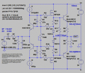
Pretty sure autobias can actually do that! Here's the output stage of my original autobias design, as posted over in the thread about it: Original thread (has the LTSpice ASC)The auto-bias circuit is very clever. I was not aware that auto-biasing was possible at audio frequencies.
However, it has a downside: the switching of D4, D5, Q3, and Q4 adds four kinks to the transfer curve. I'll call this "auto-bias distortion".
I like to design amplifiers with good open-loop linearity. I don't think auto-bias can do that.
Ed
Since this version of the amp has the current sense resistors in the output transistors' collectors (instead of at the emitters), no semiconductors in the signal path ever switch. Only the clamping diodes do switch (very softly), but they're in the collector paths, so they don't influence the output voltage at all. No transistor ever turns off.
Here's the output stage's transfer function with a linear ramp at its input and no feedback other than the auto-bias:
No kinks at all driving a 4 Ohm load.
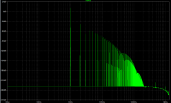
Here's the distortion spectrum of just the output stage shown above, driving 10Vpp into 4 Ohms - again, no feedback:
Harmonics are 50dB down. And that's in a class-AB Darlington output stage without feedback, operating entirely open-loop, except for the autobias circuitry.
It gets a lot better when you operate this design in closed-loop, of course: LTSpice distortion simulation in the original thread
Attachments
Last edited:
Moving the sensing resistors/diodes to the collectors greatly reduces the non-linearity, but does not eliminate it because the collector voltage still changes (slightly). While Q6 and Q8 may not cut off, they come close.Since this version of the amp has the current sense resistors in the output transistors' collectors (instead of at the emitters), no semiconductors in the signal path ever switch. Only the clamping diodes do switch (very softly), but they're in the collector paths, so they don't influence the output voltage at all. No transistor ever turns off.
The distortion simulation is impressive. I suspect that the auto-bias distortion is being made smaller than the distortion caused by the exponential relationship between current and voltage. That could be considered to be "good enough".
Ed
@IanHegglun
Hans Polak shared ML33 adaptive bias in The Black Hole... #8472. Seems operable without thermal compensation and simpler than #167.
Hans Polak shared ML33 adaptive bias in The Black Hole... #8472. Seems operable without thermal compensation and simpler than #167.
Attachments
- Home
- Amplifiers
- Solid State
- Towards a wideband non switching Auto Bias power amp