Wow, forgot I started this one ")
I think, for now, I will make a 1-channel prototype of the circuit I intend to build, and test it with just a cap in the feedback path. If that works "good enough", perhaps with an offset adjust pot.. i will leave it at that. I can also rig up a small piece of Veroboard with a servo on it to try, i guess.
I think, for now, I will make a 1-channel prototype of the circuit I intend to build, and test it with just a cap in the feedback path. If that works "good enough", perhaps with an offset adjust pot.. i will leave it at that. I can also rig up a small piece of Veroboard with a servo on it to try, i guess.
An opamp is a reliable part. The failure rate is zero compared to the power amp itself. The only thing you have to think of is that the opamp is driven with lower voltage than the main amp. Therefore you must make some considerations both in protection but also in dimensioning the servo.jtcc1015 said:peranders,
very much appreaciate your help. I will look into the LTSpice. I have actually thought of adding a speaker protection circuit before I connect the DC servo because I understand the fact that an Op-amp circuit can have higher failure rate than a simple RC filter. Therefore, I am working on both upgrade kits simultaneously.
anatech & forr,
interesting idea, I shall look into that.
perander,
Good suggestion, I shall add some protection to the input of the DC servo. Have tried out the LTSpice simulation with the Leach Amp feedback circuit inserted and confirmed that low-pass filter on the output of the DC servo is not necessary after all. The existing filter will do the job of filtering high frequency noise from the DC servo as well.
On the other note, from the what I've heard from other DIYers who has been using the DC servo in their power amp:
I quote "The DC servo do not only correct the DC offset condition on the output of my power amp, but also, depending on which Op-amp is being used, slightly changes the original sonic character the power amp itself.
To me, this is perfectly understandable as different Op-amp do perform differently in a given environment, and this is the "side effect" offered by the DC servo that I am also insterested to explore. Well, it may sounds like witch-craft to someone while unorthodox to others, but it does provide a very convenient way to teawk the sound character my power amp.
jaycee,
welcome back. Yes, you are the thread starter, I have no intention to steal it from you. Just that, I am in the verge of implementing a DC servo kit onto my Leach Superamp and got anxious to hear opinions and suggestions from your goodself and others.
I shall look forward to your further updates on your project.
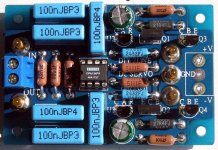
BTW, I have just done soldering the boards. Attached is the photo of the one them:
interesting idea, I shall look into that.
perander,
Good suggestion, I shall add some protection to the input of the DC servo. Have tried out the LTSpice simulation with the Leach Amp feedback circuit inserted and confirmed that low-pass filter on the output of the DC servo is not necessary after all. The existing filter will do the job of filtering high frequency noise from the DC servo as well.
On the other note, from the what I've heard from other DIYers who has been using the DC servo in their power amp:
I quote "The DC servo do not only correct the DC offset condition on the output of my power amp, but also, depending on which Op-amp is being used, slightly changes the original sonic character the power amp itself.
To me, this is perfectly understandable as different Op-amp do perform differently in a given environment, and this is the "side effect" offered by the DC servo that I am also insterested to explore. Well, it may sounds like witch-craft to someone while unorthodox to others, but it does provide a very convenient way to teawk the sound character my power amp.
jaycee,
welcome back. Yes, you are the thread starter, I have no intention to steal it from you. Just that, I am in the verge of implementing a DC servo kit onto my Leach Superamp and got anxious to hear opinions and suggestions from your goodself and others.
I shall look forward to your further updates on your project.
BTW, I have just done soldering the boards. Attached is the photo of the one them:
Attachments
anatech ,
"forr is hit on something I have noticed over the years. If an amplifier is balanced and the diff pair doesn't have to do much work to maintain a DC balance, the amp sounds much better. I didn't know why that was until having the time to study this in the last few years. A DC servo circuit may interfere with the diff pair, throwing the collector current balance out."
jtcc1015
"anatech & forr,
interesting idea, I shall look into that."
I think the complementary differential input is fundamentally a wrong concept because, among other things, each input differential creates its own offset at its output and the two offsets of the upper and lower differentials can never be fully equal in value. Particularly in this case, a servo fed back to the Vas à la Perrot should do better than one fed back to the input.
~~~~~~~ Forr
§§§
Hi forr,
I agree, I have never liked the sound of amplifiers using complementary differential pairs. I have found they sound a whole lot better when all the diff pairs (NPN and PNP) are matched to the same DC beta. They will not operate perfectly equally as pairs, but that's better than the normal mis-matched mess I see.
-Chris
Hi Greg,
The best way to balance that circuit is to match all the transistors together, and the current sources. That I think gives you the best sound quality possible from this configuration. Over 20 yrs experience with doing that.
The only problem is, I don't think it sounds very good compared to a single diff pair. I'll trade 10~30mV DC offset for a balanced differential pair any day.
Hi Leolabs,
Duo-beta (Luxman term) is a DC servo in any design I have seen, unless I am thinking of the wrong thing. It works by unbalancing a diff pair to correct for the natural DC offset.
-Chris
Hi Anatech,
My dual diff'ls are always beta matched to < 5%. And they use the above DC offset adjust cct (patent pending). the beauty is that there is no need to filter supply lines - just the trimpot and a resistor - couldn't be simpler or work better. It can even be used for AC coupled so zero any DC to < 1mV.
This is what I call simple elegance folks.
Cheers,
Greg
PS wait a moment - doesn't a Leach have dual diff'ls ( and they sound no good - watch for the wrath of GOD, Anatech). Could it be we can improve it with this cct?
jaycee said:Is it worth the extra effort of using a DC servo on an amplifier ?
If the power amp. you've just designed needs a servo, or a pot. to trim DC offset, scrap the design and start again....

Hi Greg,
If you match your pairs, as I do, there is no need at all for the balance control (as Mike has pointed out). Your balance control will operate by messing with the current densities of the two pairs.
Many amplifiers use the complementary diff pair. I don't like the sound of any of them. The early Brystons are one example. To improve, all you need to do is match the DC beta of all four transistors and thermally couple them. DC offset becomes less than 5 mV typically. Not enough to worry about by anyone's standards. Your control seems to be redundant to me. Please correct me if I'm wrong.
(But if you must, it's a cool way to do this).
-Chris
Hi Anatech,
Of course my matched beta comp diff'l inputs don't need it - in AC mode DC offset's < 2mV typ. but if DC mode is used the DC at the main input is then multiplied by the amp gain. 28 times in my case. That makes 1 mV -> 28mV. To equalise that out requires an identical 1mV at the inverting input which is 1K to ground so a current of 1uA is required from the 'cool' network. That's 1uA through 100K = 0.1V which, with a 100K trimpot is a 30deg rotation off centre roughly. Since the input stage is also degenerated by 11mV ( 500uA across 22R each) then the 1mV alteration at the inverting input constitutes < 10% change in diff'l currents.
Worth doing ? If not just leave it centred , then it only draws 12uA from both current sources, with no imbalance of the diff'ls.
People like to null offset for all sorts of reasons. Maybe a triamped tweeter direct feed.
Cheers,
Greg
Hi Greg,
I would not tend to worry about 28 mV worth of offset, since you have DC gain. The danger is a tech not understanding how these work when doing a repair.
I can see why you included it. Just to get the number down if nothing else. How much difference did you notice compared to using a cap to kill DC gain?
-Chris
Re: Re: To use DC servo or not?
Good advice. How is your approach then in partical terms?mikeks said:If the power amp. you've just designed needs a servo, or a pot. to trim DC offset, scrap the design and start again....
Negligible offset by design
Hi Mikeks,
I too, would like to see how it's done BY DESIGN rather than matching components.
Hi Mikeks,
If the power amp.......needs .........a pot to trim DC offset, scrap the design and start again....
I too, would like to see how it's done BY DESIGN rather than matching components.

Gentleman,
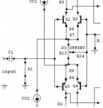
Can you please take a look at the attached shematic?
In order to get no imbalance in currents in the diff legs:
*I put a pot in one of the current sources to bias the zeners for the cascode. This works pretty good in simulation. By adjusting the pot, I also will influence the current running througth the oppossite diff pair. --> current in both legs of the diff will be equal.
*I did some sims with input voltage and frequency changed. --> the output offset had a maximum of +-60mV. But I will use a DC servo. Here I also would like to have the currents in both diff legs equal. So, with an opamp (V7 in shematic), I'll influence the reference voltages (R3 + R29) for the current sources.
With a dual complementary differential, imbalance in currents throught the legs will have more influence than with one dif, I think? Not?
With these resistor values (R74=100K), I can have DC offset of about 0.95V worked away. The current flowing througth the opamp output (R74) is about 280nA??
I once saw a shematic where the current sources also where influenced by a servo --> from there the idea offcourse. One mayor advantage is that output- and input filters from the servo are much less critical.
How do these values look to you? What do you think about the principle?
Greetz
Ben
Attachments
anatech said:My thought is that it has to be better than a large electrolytic with very little bias across it. If your circuit is relatively stable you can offset the DC offset with a pot and DC potential lke they used to do it.
Actually, you are forgetting about several factors. What you really want is to be able to not affect the output stage in any (significant) way, as well as not altering the operation of the amplifier in any way, including noise and harmonic spectrum, above 1.375Hz or even 0.3Hz. The former frequency is one decade below the lowest frequency that is perceived as a single tone, rather than discrete pulses, and the latter frequency is one decade below a generous room leakage frequency (the walls, paint, etc. start to act as a highpass filter at about 3-5Hz in a normal house).
One idea that I'm planning on using for the next amp in my pipeline (a power amp for a friend of mine) should handle this nicely, I hope, through generous use of various types of FET devices.
I'll try to explain the topology I've been considering so far:
The input consists of an input transformer (Lundahl LL6404 Zero-Field transformer), driving the input stage in common gate mode. This transformer has an exceptional bandwidth, and is intended for this mode of operation, which yields near-DC performance.
The input stage is a fully complementary differential JFET stage using four highly linear low-noise complementary matched JFETs (with NP0 caps for equal Ciss/Crss between N and P devices) and four cascode devices per channel, plus one transconductance resistor, four self-bias resistors, four gate stoppers, eight I/V resistors plus 4 NP0 caps (for bootstrapped connection to the VAS stage) and two bootstrap resistors (to not load the voltage feedback network at AC). I will add an NP0 cap across the transconductance resistor and/or the source resistors if the stage has its open loop F3 any lower than 2.5MHz. I may also decide to paralell several input devices here, as capacitance is a non-issue, whereas noise is not.
The input stage, having the best PSRR (>100dB), CMRR (>120dB) and gain (>40dB), is protected from clipping and latch-ups by DPAD diodes (dual Ir<1pA Vf<1.5 (0.8typ) diodes, preferrably from Linear Systems).
Feedback is delivered to the regular voltage inputs through identical low-impedance voltage dividers, while the signal is delivered common-gate. That insures that both halves of the circuit will see the same impedance and same common mode signal, without any imbalances.
Also, the low, identical impedances at the voltage inputs will leave no room for DC imbalances caused by unequal gate leakage currents, and those are on the order of femtoamperes to picoamperes anyway.
The VAS stage is also a fully complementary differential JFET stage, using four cascoded low-noise bipolar current sources, four highly linear high-current low-noise complementary matched JFETs (with NP0 caps for equal Ciss/Crss between N and P devices) and four cascode devices per channel, two transconductance resistors, four self-bias resistors, four gate stoppers, one I/V resistor plus four Vgs bias trimpots, and four bootstrap resistors (to not load the input stage at AC). The NP0 caps are connected from between the two I/V bootstrap resistors of an input stage leg and the source of the corresponding leg of the VAS stage; this makes the I/V resistors behave more like current sources in the interesting range. Similarly to the input stage, the transconductance resistors will be individually compensated (for proper Gm balance) to match the open loop F3 of the input stage exactly, erring on the side of speed (it's generally better for the stages to be progressively faster, according to at least GamuT).
The output stage is (surprise) a fully complementary differential/bridging compound follower stage, using four Exicon 10N16 lateral VFETs, four 0.1R bias resistors, four OnSemi output bipolars with thermal tracking, four compound bias resistors (connected through the tracking diodes for perfect bias), four NP0 bypass capacitors (for the tracking diodes), four emitter degeneration resistors for the bipolars, four base stoppers, four gate stoppers, four NP0 bypass caps to compensate the N-ch/P-ch Ciss difference and dwarf its nonlinear characteristic, two 0.05R output series resistors (to isolate the load), caps across the load and from load to rails (2.5MHz lowpass to avoid RF injection through the feedback path), soft recovery blocking diodes, 1Kohm dummy load and zeners across the load. Feedback is taken from the inside of the 0.05R isolating resistors, to avoid instabilities. The damping factor will still be dominated by the cable in many/most cases.
Depending on the slew rate of the output stage, I may decide to use a bootstrapped, cascoded complementary JFET buffer to drive each VFET. The added open-loop distortion should be in the ppm range, 2nd and 3rd harmonic only, if the right devices are used.
The voltage across the 0.1ohm resistors is buffered, lowpassed and used to drive the current sources in the VAS stage; one current source in each VAS leg and, hence, to each output leg. That way, I get to accurately set the current in each output leg.
The VAS gain devices themselves will be matched complementary JFET devices, except for the current sources (which will be dual precision matched bipolars with cascode operation) operated at their measured zero-tempco point. That way, the VAS remains unconditionally stable, with at most a few microvolts of open-loop offset.
The input will similarly be using matched complementary JFET devices, presumably dual monolithics like the LS843's, again limiting open-loop offset to the order of microvolts.
All the fets have source resistors and are biased in the manner suggested by Vishay Siliconix. This further lowers the 1mv(max) Vgs difference of the LS843's to microvolts over the transconductance resistor.
The power supply will use seperate transformers per stage (more important than dual mono, IMHO). Input and VAS stages get CRCRC filtering, output stage gets CLC filtering. Input and VAS stages get per-channel DC+AC series pass regulation. Output stage gets very low frequency low-drop AC series pass regulation per output leg per channel with a constant voltage relative to the output (effectively a cascoding supply). All stages get active high-frequency shunting using JFET/DMOS shunts (you can easily get GHz-range filtering, though lateral DMOS' are really twitchy), and local RC decoupling.
All the protection circuits are essentially implemented in the series pass power supply; that is, heat sink temperature, current draws that are more than 60 degrees out of phase with the output voltage, SOA protection, etc. Fan control will also be implemented here; this thing can get hot, despite my plans to run the Exicon's with low bias, and the OnSemi's near class B. I just have to figure out the correct way to transition them without running into Gm-doubling problems and/or crossover distortion.
Also, I may end up swapping at least some of the NP0s for PTFEs, etc., but that comes later.
I'm still fine-tuning the circuit before breadboarding the stages, so no diagrams yet, but I think it should give you some ideas as to how you can get a REALLY low DC offset. At lower powers, it should be even easier.
Bear in mind that you are still free to start trimming the circuits to get into the nanovolt-picovolt offset range

It's always important to put things in perspective like is it important the distortion spectrum caused by the DC-servo in the 0.3-1.375(!) Hz? I can't see how you effect the output stage by a 100k-1M load??angel said:Actually, you are forgetting about several factors. What you really want is to be able to not affect the output stage in any (significant) way, as well as not altering the operation of the amplifier in any way, including noise and harmonic spectrum, above 1.375Hz or even 0.3Hz. ...

- Status
- This old topic is closed. If you want to reopen this topic, contact a moderator using the "Report Post" button.
- Home
- Amplifiers
- Solid State
- To use DC servo or not?