View attachment simpleP-sourcefollower-Zenitron-1.asc
This is just an idea. I have not really tried to optimize anything. I just wanted to get a general feel for the function and ballpark potential performance from this simple circuit.
I am sure there are better more suitable devices. And the amp seems to really like lots of current running through the fets (less THD).
If you would replace the 10R resistors with current sources. you could reduce the voltage to 15V without performance loss.
Ultimately the maximum output is limited by the Vgs of the device.
There aren't many that has Vgs >5V.
And the high capacitance will make life difficult for the signal source.
Interesting nevertheless,
Patrick
Ultimately the maximum output is limited by the Vgs of the device.
There aren't many that has Vgs >5V.
And the high capacitance will make life difficult for the signal source.
Interesting nevertheless,
Patrick
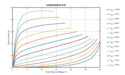
I ran the UJ3N065080K3S through the curve tracer to see what the curves look like in reality, as the datasheet curves do not cover the typical "audio amplifier range" very well; see attachment. The flattening of the curves at high current is due to the self heating and negative tempco. However, I am not sure what's happening at 20 V and higher... is this normal for a JFET? What is it?
My opinion is that the device is a SIT at low-ish current and high-ish voltage and has triode-like behavior in this region.
At low-ish voltage and high-ish current, the device is an ordinary power JFET with petode-like behavior.
The intended application for this device is a power converter/inverter. The device is used as a switch. The device is either totally off or extremely on. The pentode region is all that the manufacturer cares about. The linear region between the on and off states is meant to be inhabited for as short a time as possible to mitigate switching losses.
I just ordered a handfull to curve trace up to 200V. My guess is that it will look like a Sony 2SK60.
The flattening of the curves that you see is the transition region between SIT behavior and normal JFET behavior.
I just ordered a handfull to curve trace up to 200V. My guess is that it will look like a Sony 2SK60.
I am looking forward to your results. I couldn't take mine higher than 30V, as they started to oscillate badly. I couln't get it stable with a 10k gate resistor, and I also cap between gate and source or gate and drain, but no luck.
I am looking forward to your results. I couldn't take mine higher than 30V, as they started to oscillate badly. I couln't get it stable with a 10k gate resistor, and I also cap between gate and source or gate and drain, but no luck.
What curve tracer are you using?
I am using programmable power supplies (Korad KWR 103) with this software: GitHub - mbrennwa/PyPSUcurvetrace: Python program for I-V curve tracing of electronic parts using programmable power supplies
I am using programmable power supplies (Korad KWR 103) with this software: GitHub - mbrennwa/PyPSUcurvetrace: Python program for I-V curve tracing of electronic parts using programmable power supplies
My day job gives me access to sourcemeters and power supplies. I did an experiment recently where I tried to use a dual-channel power supply to characterize a MOSFET from the front panel the way I do it with a dual channel sourcemeter.
The result was a failure. My guess is that the programmable power supply has noise garbage that causes the problem.
My suggestion to you is to record where you were experiencing oscillation and then use the front panel of the power supplies to look at that operating point with an oscilloscope. Then construct some RC or LC filters to try to cure the oscillation problem.
My suggestion to you is to record where you were experiencing oscillation and then use the front panel of the power supplies to look at that operating point with an oscilloscope. Then construct some RC or LC filters to try to cure the oscillation problem.
That's exactly what I did. No luck.
That's exactly what I did. No luck.
From your description I would call what you did is to use a gate stop resistor and a snubber.
I am guessing that you may need a ladder network of RC elements.
If you have access to a spectrum analyzer, that will tell you at what freq the oscillation happens. You can construct the filter accordingly. Otherwise you are shooting in the dark.
A spectrum analyser is not needed. I can see the oscillation on the scope, and I could take the frequency from there. I would think that all I need is a (series of) RC filters that cut off above 50 Hz or so, since the programmable PSUs are pretty slow anyway. I might try harder if I get the time.
A spectrum analyser is not needed. I can see the oscillation on the scope, and I could take the frequency from there. I would think that all I need is a (series of) RC filters that cut off above 50 Hz or so, since the programmable PSUs are pretty slow anyway. I might try harder if I get the time.
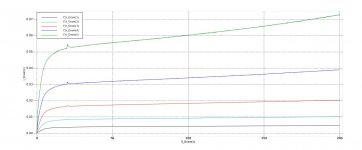
I set up a 2SK60 on the sourcemeter and measured Igs at Vds =25V and Vgs=-11.5V and Ids is 1mA. This is nominally the SIT threshold condition.
Igs is ~1nA. This makes the apparent input impedance ~10G ohms. My thinking is that a 10k gate stopper will have no effect. Maybe try different values between 1M ohm and 10G ohms as a gate stopper. That will likely create a voltage divider and change actual Vgs which you will have to account for. Its just an idea for an experiment.
United SiC JFET
This is the depletion mode SiC JFET. It shows no SIT behavior. It does how self heating even though I am using 0.03 NPLC which is 500uS per point.
It has a positive tempco and looks fairly non-linear. The Vgs spread on these curves is 0.35V total.
This is the depletion mode SiC JFET. It shows no SIT behavior. It does how self heating even though I am using 0.03 NPLC which is 500uS per point.
It has a positive tempco and looks fairly non-linear. The Vgs spread on these curves is 0.35V total.
Attachments
Interesting! However, I am not sure I am looking at this correctly... what are the different curves? The legend seems to imply different drain currents, but I guess that's not right.
Also, could you go to (much) higher drain currents?
X-Axis is drain voltage. It goes to 200V. Y-axis is drain current and it goes to a bit above 70mA. The different curves are different fixed negative Vgs values.
Yes I can go to much higher drain currents. My interest was to see if there is any SIT-ish behavior of the kind exhibited by the LU1014D. The 2SK60 also behaves similar to the LU1014D.
I can see from the little bit that I did with this United SIC part that the tempco behavior will dominate the curve tracing. It may be able to be mitigated with some heatsinking and some faster pulsing.
That said, I do not see this device showing anything at high currents than what you can already see in what I posted.
Exactly what are you looking to discover?
My opinion about this family of curves that you traced has changed.
My opinion now is that the device has an extreme positive tempco at low-ish current and a negative tempco at high-ish current. This causes the false SIT-ish looking curves that you traced.
This makes sense from an application standpoint. SiC FETs are used as a switch to be operated at high current at high temp. If the tempco there is negative, the device will have less tendency to experience thermal runaway. The manufacturer does not care about the tempco at low current at low temp.
Here is an experiment. Mount your SiC device to a heatsink. Also mount a garden variety MOSFET to that heatsink.. Use the garden variety FET as a heater get the heatsink to 50 deg C. At this high temp, perform your power supply curve tracing. You should see normal pentode curve traces.
Attachments
I thought the same, but I am not sure. Take a look at the datafile in post 136, and you'll see that the SiC was idling at 60 Watt for 10 seconds between each reading. This means the SiC was running quite hot throughout the entire test, not just in the "triodey" area.
I feel we're getting very off topic here...
I feel we're getting very off topic here...
I thought the same, but I am not sure. Take a look at the datafile in post 136, and you'll see that the SiC was idling at 60 Watt for 10 seconds between each reading. This means the SiC was running quite hot throughout the entire test, not just in the "triodey" area.
I feel we're getting very off topic here...
I will start a new thread for the United SiC device.
I have a suggestion. Start your sweep at the highest voltage and sweep to the lowest voltage. Try it first with no delay between measurements. I think you may see that there is no "triodey" area.
- Status
- This old topic is closed. If you want to reopen this topic, contact a moderator using the "Report Post" button.
- Home
- Amplifiers
- Pass Labs
- The Zenitron