i notice in the guide you recommend rinsing with soapy water, i use noclean flux, so dont always do this, but when i do i use distilled/demineralised water, not so important with plain SMD resistors and ceramic caps, but for the opamps and other ICs i always take this precaution
nice work on the guide though mate!! i think it illustrates well how easily it should come together, i think its great that some of the anti-smd mythology is being combatted
@qusp, I was sure there was to be more gibes about the lighting in the pics!
@opc, thanks for the guide wiki! I read the sections about bal-se and all made sense. Having never had a good excuse to try smd before the guide and the video have given me more confidence in pulling these builds off without too much hassel.
 i find the main difficulty with SMD is if there is troubleshooting that needs doing, because you cant just lift one leg of a resistor.
20v hybrid Wire
It would actually be possible to build a 20V "hybrid" Wire, something I'm thinking about doing with one of my SE-SE boards, using the LME49610 and LME49860 chips. Both are rated for a maximum of 44V (+/-22V rails).
http://www.national.com/profile/snip.cgi/openDS=LME49610
http://www.national.com/profile/snip.cgi/openDS=LME49860
lme49610 - Octopart
lme49860 - Octopart
The LME49610 is just the high(er) voltage version of the LME49600 and just replaces that chip on the Wire PCB. The LME49860 is a dual low-distortion high(er) voltage audio op amp. To make it work with the SE->SE board both LME49990s would be left off, along with R13 - R20. Pin 3 would be shorted to pin 6 on the 49990 pads and R13 & R17 jumpered. Those changes run the inputs of the LME49610s right to the input of the SE->SE PCB. The 330uF caps also have to be bumped up to 25Vdc units.
Then an LME49860 would be wired up on an external PCB, either the DIP or SOIC version with R13 - R20 resistors wired similarly to the SE->SE board. Then the outputs of the LME49860 go to the inputs of the SE PCB, and the output of each LME49610 wires back to R16 and R20 as with the original board to complete the feedback loop around each buffer.
Finally the whole thing gets powered by a +/-20Vdc power supply. The Wire power supply could probably be altered to produce 20Vdc by changing the set resistors R30 & R32 appropriately, along with upping the working voltage of the capacitors accordingly and using an 18 - 20VAC transformer.
And just like that you have a 20V Wire! +/-18Vdc would be another interesting rail voltage to run it at, and probably more practical. The LME49610 datasheet shows a maximum voltage overhead of about 2.5V. Assuming the datasheet is lying, which I always do (!), lets assume 3V. +/-18Vdc rails then would support a maximum swing of around 18V - 3V = 15V, or 10.6Vrms. Into 600R headphones that would be [(10.6) ^ 2 ] / 600 = 187mW. With 20V rails you get a maximum swing of 17V and 241mW out into 600R, which should be enough for just about any 600R cans on the planet!
Interesting to note that the current draw is minimal into the high z cans, almost what the LME49860 can handle itself. 17V peak swing gives 28mA peak, or 20mA rms into the 600R load. That is with sine waves too. Music power would be considerably less.
The net result would definitely have reduced measured performance on opc's AP due to the LME49860 vs. the LME49990 specs, the dual op-amp vs. two singles, the off-board parts, the extra wiring, the wiring lengths between the two PCBs, etc. Whether the difference would be audible though I don't know.
Hi OPC (and all other interested!)
Provided I use electrolytic caps with a higher voltage rating, do you think it would be harmful in any way to power the Wire at +/- 17V instead of 15V (or 12V) as recommended (stability, heat, anything else)? For me the only issue might be fitting the larger capacitor on the tight board...
The reason is to simplify power supply efforts (semi-long story) but I'll be using a similar LM317/337 power supply to the one designed by OPC, only it is running at +/- 17V
Thanks for your thoughts in advance!
PS OPC, I'm not yet in green on the PDF, but crossing my fingers for an xmas miracle
It would actually be possible to build a 20V "hybrid" Wire, something I'm thinking about doing with one of my SE-SE boards, using the LME49610 and LME49860 chips.
Both are rated for a maximum of 44V (+/-22V rails). http://www.national.com/profile/snip.cgi/openDS=LME49610
http://www.national.com/profile/snip.cgi/openDS=LME49860
lme49610 - Octopart
lme49860 - Octopart
The LME49610 is just the high(er) voltage version of the LME49600 and just replaces that chip on the Wire PCB. The LME49860 is a dual low-distortion high(er) voltage audio op amp. To make it work with the SE->SE board both LME49990s would be left off, along with R13 - R20. Pin 3 would be shorted to pin 6 on the 49990 pads and R13 & R17 jumpered. Those changes run the inputs of the LME49610s right to the input of the SE->SE PCB. The 330uF caps also have to be bumped up to 25Vdc units.
Then an LME49860 would be wired up on an external PCB, either the DIP or SOIC version with R13 - R20 resistors wired similarly to the SE->SE board. Then the outputs of the LME49860 go to the inputs of the SE PCB, and the output of each LME49610 wires back to R16 and R20 as with the original board to complete the feedback loop around each buffer.
Finally the whole thing gets powered by a +/-20Vdc power supply. The Wire power supply could probably be altered to produce 20Vdc by changing the set resistors R30 & R32 appropriately, along with upping the working voltage of the capacitors accordingly and using an 18 - 20VAC transformer.
And just like that you have a 20V Wire!
+/-18Vdc would be another interesting rail voltage to run it at, and probably more practical. The LME49610 datasheet shows a maximum voltage overhead of about 2.5V. Assuming the datasheet is lying, which I always do (!), lets assume 3V. +/-18Vdc rails then would support a maximum swing of around 18V - 3V = 15V, or 10.6Vrms. Into 600R headphones that would be [(10.6) ^ 2 ] / 600 = 187mW. With 20V rails you get a maximum swing of 17V and 241mW out into 600R, which should be enough for just about any 600R cans on the planet! Interesting to note that the current draw is minimal into the high z cans, almost what the LME49860 can handle itself. 17V peak swing gives 28mA peak, or 20mA rms into the 600R load. That is with sine waves too. Music power would be considerably less.
The net result would definitely have reduced measured performance on opc's AP due to the LME49860 vs. the LME49990 specs, the dual op-amp vs. two singles, the off-board parts, the extra wiring, the wiring lengths between the two PCBs, etc. Whether the difference would be audible though I don't know.
Last edited:
Hi Guys,
Thanks for the comments so far! I do apologize about the poor lighting... I suppose photography is not my calling in life. Perhaps the shadows from the parts are a comment on modern society. Did any of you think about that
I'll update that wiki as people start building and I get feedback. The main purpose is to put people at ease about the SMD thing. It's really not that many parts to solder, and I think most people will realize that it's much easier than they may have been thinking.
qusp:
The copper on the top layer for the BAL-BAL version is about 0.85" square. The SMD heatsinks add another 1.85" square for a total of about 2.7" square per device.
Keep in mind that the top mounted BGA sinks are not really all that effective since the thermal resistance from the die to the top of the TO-263 pack is massive. The SMD heatsinks sidestep that issue by connecting directly to the copper that the tab is soldered to making the whole system pretty efficient at getting the heat out.
On the bright side if you're running less than +/-10V rails with the BW pin floating, there's not really a need for heatsinks at all. The idle dissipation on that board would be right around 1W for the entire board and the majority of that is actually the OPA1632.
You'd be better off finding a really thick TIM like this:
Gap Fillers - heatsink interface material
And finding a clever way to heatsink directly to whatever metal case you might be using.
Cheers,
Owen
On a side note, while searching for the LME49600 datasheet I notice that TI has finally put thier cover page over the datasheet. I really hope that acquisition turns out for the best!
Last edited:
haha hey Owen, i actually think the pics are perfectly fine, very good even, my only comment was a half joke related to the SMD soldering vid you posted a while ago; at least i assume thats what hochopeper was referring to. dont take it to heart, i'm just being my usual annoying self =)
thanks for that mate, yeah i'll be testing without sinks first and that interface material is perfect if that doesnt cut it, considering the case will be CNC i'll be able to design to allow it to interface fairly well and considering all other heatsinking in the build is taken care of by copper pour it'll hardly get warm. i'm just slightly concerned that i wont be able to go without a heatsink on the buffers due to the really low impedance headphones i'm using and there isnt enough vertical room for the ones in the bom i dont think. thats the main reason i asked for the headamps to be sent ahead.
I might still use the BGA sinks on the top side as there is unlikely to be a way i can interface to the floor and the roof, plus they look cool
the opa1632 always run a little hot, thats why i recommended the DGN version or the option for it, but its not conducive to first time SMD builders and requires a VIA under the power pad to be hand soldered.
re the Ti takeover, yeah i saw that too when researching the lme49713, i agree its a worry, national datasheets were always better as far as app notes IMO, heres hoping they now offer the same samples scheme on the national chips as Ti, having to pay multiple shipping charges for multiple parts that end up being shipped together is a bit of a pain.
Last edited:
Owen, when you say "rubbng Alcohol" do you mean isopropyl alcohol (isopropanol) or ethyl alcohol (ethanol).
I mostly use aerosol Isopropanol (a.k.a. IPA).
Have used some the Fluxcleaners, eg, Chemtronics Flux-Off, though only in a well ventilated area.
Did you get my PM's.
Thanks.
I mostly use aerosol Isopropanol (a.k.a. IPA).
Have used some the Fluxcleaners, eg, Chemtronics Flux-Off, though only in a well ventilated area.
Did you get my PM's.
Thanks.
Last edited:
Hi Guys,
Thanks for the comments so far! I do apologize about the poor lighting... I suppose photography is not my calling in life. Perhaps the shadows from the parts are a comment on modern society. Did any of you think about that
Nothing to apologise for opc, the photos show everything perfectly. I was having a dig at qusp more than anything!
I'm trying to decide on an optimal arrangement now for my The Wire BAL-SE setup.
Will be fed directly from output of TP Opus (WM8741) DAC. I'd like to get RCA and headphone outputs. As I see it there is a few options:
A) RCA and headphone ports in parrallel off the board.
B) Relay switching between headphone and RCA outputs.
C) Dual 'The Wire' BAL-SE in parallel off DAC.
D) Relay switching between two BAL-SE 'The Wire' off DAC.
Taking into consideration length/impedance of wires connecting these up I'm personally leaning towards relay switching outputs per option B. Thoughts?
screw that!! relays will add resistance/impedance at the output and the decent ones are often of limited current capability
as long as the wires are kept short, just run them in parallel from the output option A. just dont leave the headphones plugged in when not in use. if you must use a switch; IMO you are better off using a high quality mechanical switch
as long as the wires are kept short, just run them in parallel from the output option A. just dont leave the headphones plugged in when not in use. if you must use a switch; IMO you are better off using a high quality mechanical switch
Last edited:
I'll echo qusp's comments... just run them in parallel at the output as in A.
No need for relays or a switch. Even if you were driving both headphones and the RCA outputs at the same time I don't think you'd notice a difference.
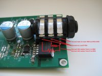
What you could do if you want a really cheap and easy "or" type inplementation (where the RCA jacks are turned off when headphones are plugged in) is to use the same jack as used on the first version of The Wire but connect a pair of RCA jacks to the switched pins on the side of the jack. These jacks are specifically designed to work as switches, but I would opt for the gold plated version if you're using it this way.
The GND pin should be hard wired to always be connected, and you'll want some 10k resistors from each output to GND to reduce clicks and pops.
See pictures for details - and feel free to comment on the excellent lighting!
Cheers,
Owen
No need for relays or a switch. Even if you were driving both headphones and the RCA outputs at the same time I don't think you'd notice a difference.
What you could do if you want a really cheap and easy "or" type inplementation (where the RCA jacks are turned off when headphones are plugged in) is to use the same jack as used on the first version of The Wire but connect a pair of RCA jacks to the switched pins on the side of the jack. These jacks are specifically designed to work as switches, but I would opt for the gold plated version if you're using it this way.
The GND pin should be hard wired to always be connected, and you'll want some 10k resistors from each output to GND to reduce clicks and pops.
See pictures for details - and feel free to comment on the excellent lighting!
Cheers,
Owen
Attachments
Last edited:
i mentioned not leaving the headphones plugged in, not because i think the load would be a problem so much, more that you would want to be running it probably at full volume for the line out, maybe not so good for the headphones 
 . that and perhaps having an aerial connected to ground at least on paper maybe not so great either. in practice the latter may not be a problem, but the former might be very expensive.
bloody oath those pics are sh1t man! Owen, i'm highly disappointed in you, poor show
. that and perhaps having an aerial connected to ground at least on paper maybe not so great either. in practice the latter may not be a problem, but the former might be very expensive.bloody oath those pics are sh1t man! Owen, i'm highly disappointed in you, poor show
ahh... good point about over-driving the headphones... I hadn't really thought about that.
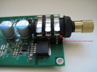
In that case, it's probably best to disconnect! The above circuit would give you a not-so-subtle reminder to disconnect your headphones, as the RCA outputs wouldn't work until you did.
No worries about the photography comments either... I'm just kidding around
Also, no comments about how dirty that board is... it was my test platform for the SE-SE variant and was never cleaned up!
Cheers,
Owen
ahh... good point about over-driving the headphones... I hadn't really thought about that.
In that case, it's probably best to disconnect! The above circuit would give you a not-so-subtle reminder to disconnect your headphones, as the RCA outputs wouldn't work until you did.
That'll work perfectly. I will be doing volume attenuation in the digital stage. These switched phone jacks will certainly be simpler and neater than any of my ideas! In my application OR is definitely the only use case, can't think of any time I'd want to run both simultaneously.
About the inner "3rd" layer of the PCB...
Hi Owen - This is slightly off-topic, but I thought I'd post in case others were interested... Are the hidden inner layers of the PCBs simply a ground plane connected to ground in a single place (presumably at the input or output), but otherwise "ducked" out of all the vias? I've only ever done 2 layer boards, and would be curious to your approach on the 3rd layer. Does it cover the entire board (except the vias of course), or did you deliberately also skip out on other areas of the board (such as under the buffer, etc).
Cheers, and as always - thanks for this amazing contribution of yours!
Hi Owen - This is slightly off-topic, but I thought I'd post in case others were interested...
Thanks for asking that absolutely on-topic question for me
- Home
- Amplifiers
- Headphone Systems
- "The Wire" Ultra-High Performance Headphone Amplifier - PCB's