Thank you oiphy.
I have seen this schematic, one of the many, no protection circuit, different power supply voltages + / - 80 V instead of my + / - 56.5 V.
Your R36 is still 0.22 Ohms instead of suggested 22 Ohms.
My first question is about the version of PCB's I have.
It seems to me that these are the changes that Liliya suggested.
Still don't understand what happens with the protection circuit I have.
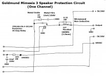
Your second picture shows Error (403)
Could you put some light over my questions please ?
Thank you again.
I have seen this schematic, one of the many, no protection circuit, different power supply voltages + / - 80 V instead of my + / - 56.5 V.
Your R36 is still 0.22 Ohms instead of suggested 22 Ohms.
My first question is about the version of PCB's I have.
It seems to me that these are the changes that Liliya suggested.
Still don't understand what happens with the protection circuit I have.
Your second picture shows Error (403)
Could you put some light over my questions please ?
Thank you again.
Attachments

Goldmund clone
owivankenobi
First of all, do not be afraid to seek advice. Here at DIYaudio, I am sure there are many helpful people ready to assist.
I choose to start with your question number 10:
If you have downloaded what oiphy have suggested, then you can compare the schema you received from Nagy (Mimesis 3) with Mimesis 9.2. Compare component to component. Some semiconductors are different, some capacitors too. In the case of the small capacitors (pF) Nagy suggest several alternative values. I see this as a finishing touch to optimize the amplifier. If you want such optimization you should have access to scoop. I initially advice you to go (mostly) for the components referred to in the schema of Nemesis 3 .
Nemesis 9.2 has, as you can, see three pairs of power FETs. The power supply is also different (higher voltage).
1. and 2: Remember that Nagy had good personal experience with both Nemesis 3 and 9.2.
I see no reason to doubt that his suggestion is quite ok. If you are unsure what output you can expect with the recommended transformer, there are several here on DIYaudio who possesses the necessary mathematics skills. Andrew, where are you?
3and 5: The downloaded circuit from oiphy works just fine with the values on the schema
4. There were many different opinions on whether 0.22 Ohm was an optimal value
(too low??). If I remember right, I decided to go for something in between:
2.2 Ohm (impossible to control now, hard to see).
6. Insert a potentiometer (1Kohm). When the optimal result is reached, measure the resistance value of the potentiometer and replace this with a resistance ( closest standard value).
7. I sought advice about exactly the same here at DIY audio: here is both my question and the answer I got:
Originally Posted by Liliya
A few years back (2006) you were contributing to a thread that was started by Suzie Jackson. You came with the following advice due to yours own experience with FETs:
"IMHO I have found that it is important to balance the speed difference between the N-chn and P-chn fets. This is best achieved I believe by increasing the N-channel gate resistor value with respect to the P-channel. You see the P-chn fet is quite a bit slower that the N-channel fet, so the n-channel fet will need to be slowed down to the same speed of the P-channel".
I have built two amps, Golmund Memesis 3 and 9 with these FETS: Exicon 10N16 and 10P16. I want to take all precautions to avoid oscillations, therefore I seek your advice about how big these resistors should be in this case. As it is now gateresistors are all equal = 100 ohms (I am aware that by increasing the value of gatemotstandene affected slew rate). Will the 100/150 ohm be a okay "combination" or should I "take the leap" and go for the 470/680 ohm??
Or somethings in between??
Regards
Eivind Stillingen, Norway
Hi Eivind
I would use 470 / 680 anything less and there would be a possibility of oscillation.
If you are using a single pair then you could drop them down to around 220 / 330, but with paralleled
pairs use the higher values above.
100 ohms for these type of mosfets is way to low.
Cheers
Anthony
Eivind Stillingen
Last edited:
Liliya , thank you again.
I trusted Nagy from the first moment. As you see, there are some touches and changes done by the forum (this was all about). It is most likely that my boards should work as they are, but I would like to collect most of the experience obtained in such a long thread and pour it over my version of the amp. I think it is reasonable.
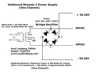
Understood, I can calculate a power supply from scratch myself, but I didn't designed the amp. This value of voltages must be specified, Nagy says 56.5 V in my papers. I have a good scope.
Of course my board does not fit a Goldmund 9 because of the 6 MOSFETS's. So I have to use 4 MOSFET's I bought.
A word about MOSFET matching procedure could be nice.
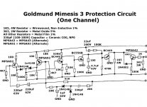
Finally, oiphy's schematics does not show the protection circuit. Please excuse my insistance about this point but I would like to be clear here: for me, this is delicate because I didn't heard of anybody saying that the Nagy board have worked if assembled as they are. My board is prepared for the protection components because I can see the Panasonic relay in it and the other related components. As you can see from my schematic version, there is no neat relation between the amplifier schematics and the protection circuit itself. It has been drafted by hand showing a modification needed for this to work that I hope it has been correctly paseed to the board. Nobody seems to report if this works, I think, maybe I missed something.
The part numbering seems to match the components of the silkscreen distribution, but I am not very sure. Why ? because my boards don't have a silkscreen printed on them, I just have a paper showing a silkscreen layer. So I guess if somebody has an schematic that includes the protection circuit as it should be, reflecting the copper of my boards. It would be nice to know that the original boards have been assembled sometime and worked fine, despite noise, MOSFET speeds and unbalancing, quiescient current isues, etc.
Finally, I don't want to bother you guys, if I don't get this answers, I will assemble one board with some smoke risks, not because of the amplifier, but I still don't feel sure about the protection.
Kind greetings to you all.
I trusted Nagy from the first moment. As you see, there are some touches and changes done by the forum (this was all about
). It is most likely that my boards should work as they are, but I would like to collect most of the experience obtained in such a long thread and pour it over my version of the amp. I think it is reasonable.Understood, I can calculate a power supply from scratch myself, but I didn't designed the amp. This value of voltages must be specified, Nagy says 56.5 V in my papers. I have a good scope.
Of course my board does not fit a Goldmund 9 because of the 6 MOSFETS's. So I have to use 4 MOSFET's I bought.
A word about MOSFET matching procedure could be nice.
Finally, oiphy's schematics does not show the protection circuit. Please excuse my insistance about this point but I would like to be clear here: for me, this is delicate because I didn't heard of anybody saying that the Nagy board have worked if assembled as they are. My board is prepared for the protection components because I can see the Panasonic relay in it and the other related components. As you can see from my schematic version, there is no neat relation between the amplifier schematics and the protection circuit itself. It has been drafted by hand showing a modification needed for this to work that I hope it has been correctly paseed to the board. Nobody seems to report if this works, I think, maybe I missed something.
The part numbering seems to match the components of the silkscreen distribution, but I am not very sure. Why ? because my boards don't have a silkscreen printed on them, I just have a paper showing a silkscreen layer. So I guess if somebody has an schematic that includes the protection circuit as it should be, reflecting the copper of my boards. It would be nice to know that the original boards have been assembled sometime and worked fine, despite noise, MOSFET speeds and unbalancing, quiescient current isues, etc.
Finally, I don't want to bother you guys, if I don't get this answers, I will assemble one board with some smoke risks, not because of the amplifier, but I still don't feel sure about the protection.
Kind greetings to you all.
this work? as attachments?
edit: got this in email from member on board here. everething worked fine for him.
quote" Hi Stig,
This amp is worth the effort.
It is the best sound that I heard him!
Transistors,resistors - Exactly like in the schematics!
R20 - 330R (biass 100mA)
T5-T6 -Contact thermal!
T7-T8-T9-T10 - Thermal contact all four together!( I did exactly as proposed by Nikos on diyaudio)
Otherwise offset will not be stable!
I'm on the board:
C3=4,7PF
C5 = 10PF
C6 = 4,7PF
C7 = 4,7PF
T7 between B-C: 4,7PF
With these capacitors is perfect signal on the oscilloscope.
Transformers : 2x50V/500W (2 bridges for channel) It is the same 2x50V /500mA for BD249/BD250
From the bottom PCB - 2x 10000/100V.
On PCB - 2x4700/100V.
Not use strong resistors in the source.
Good luck !
Excuse my English
Best regards,
Vitali
Attachments
Last edited:
Golmund clone
Unfortunately, I have not understood what is your problem regarding the protection circuit. When it comes to PCB, you are the first member I know of that use Nagys PCB. I think "all others" have used Alexs PCB.
I've looked at is your "silkscreen" that you don’t have on your PCB, but as a printed copy:
When it comes to the part of Nagy PCB, which we refer to as the protection circuit, this is exactly equal to the silk screen on my two PCB from Alex. Component values are also exactly the same. The only differences I can see is that Nagys copy have not given you the orientation for the ELE (C1-5 and C8).
The protection circuit works equally well on both my two print even if the voltage is significantly lower on Memesis 3.
My Memesis 3 is a copy of my Memesis 9.2 with the exception of three things:
1. Memesis 3 has a lower supply voltage.
2. Memesis 3 has 2x 2SK170 BL instead of 2N5564/65
3. Memesis 3 have as 9.2, three pairs of output FETs
Eivind Stillingen
Eivind I can perfectly understand what you can't understand
I have some years experience with electronics and one of my many defects is that I need that everything is clear before aseembling, circuits, PCB's and part numbers.
Please tell me if you have seen this pictures of my board before
Please understand that after so many versions of nice boards seen here, I can doubt a little. Believe me I don't like smoke
After 6 or 7 beautiful versions of other kind of boards in the thread, Nagys posts and reveals the protection circuit at post #245 and talks of the Panasonic relay at post #256.
Most of his originals has been removed from the thread
All of your kind advices and oiphy's refer to a different amplifier, now I see that it is Goldmund 9
Your last post is the first time that somebody explains the differences between the 2 circuits, considering that the intention was to clone a Goldmund 3. Thank you for that, because I have never seen this Goldminds before, and many people here own one or has cloned one. Not my case.
So I will keep on researching the thread and try to resume a little.
The part numbering is different in my "silkscreen" . I mean the paper I have, not a real silkscreen that as you can see from the attachments, does not exist. My worry is that the paper could be different from my board silkscreen.
The power supply is + / - 56 VCC if you see the attached shematic. You guys always talk + / 80 VCC, this is confusing and may bring smoke. A little advice here should be nice. Nagys also talks 80 V, I think that the is talking 56 VAC x 1.41 = 80 VCC , right ?
Now that you have explained all this, I will try to assemble my board.
Thank you for your patience but I hope that yo will understand.
Roberto Berner
Attachments
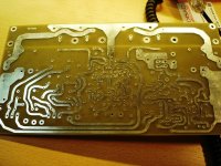
oiphy I appreciate your post, but please consider that I have the boards for a definite protection circuit
There may be lots of good protection circuits, but I should use the original one. I don't like to cut traces, this is not good practice specially in a high end device.
I need to know about the one that fits my board, please see all of the documentation that I have uploaded and that are my originals from Nagys.
Thank you
Roberto
Golmund clone
oiphy:
''''T7-T8-T9-T10 - Thermal contact all four together!( I did exactly as proposed by Nikos on diyaudio)
Otherwise offset will not be stable!'''
TRUE
Also in my amplifier C7=4.7pf must fit to T7 not T8 for best results
and leave out the capacitor on T10. Μimesis 9.2
All these measurments with full load 8Ω
Last edited:
Goldmund clone
Maybe I now creates more confusion, but my intent is the opposite:
I have looked at the thread "The very best ..... This thread started as a project that intended to clone Goldmund Nemesis 9.2, and with Nagy as the initiator.
After much controversy Nagy left this thread from the post 1147 and starts its own thread, this one: http://www.diyaudio.com/forums/solid-state/174468-very-best-amplifier-i-have-ever-heard-115.html
While leaving the Nemesis 9.2 thread, Nagy started a new project with Nemesis 3.
In one of the posts Nagy wrote that “Nemesis 3 is 95% similar to Nemesis 9.2”. As far as I can see this was the main differences:
Nemesis 3 worked at a lower voltage.
Nemesis 3 used MPSA 43/93 instead of BSS71/74
Nemesis 3 used a different print, but for me, virtually identical to the proposal from Alex and offered to DIYaudio members by Bigpanda ( small differences described later)
Both Nemsis 3 and Nemesis 9.2 uses the same “Secret circuit” with exactly the same components, but fitted with different voltage. This is perhaps one of the things that has confused obiwankenobi
In the downloaded form the “Secret circuit” from oiphy and from Nemesis 9.2 shows a voltage supply of + / -80 V DC. But the circuit works very correctly at lower voltages. This I know from my own experience with my own Nemesis 3. (I have some mistakenly given this amplifier the name Nemesis 3, but it is in reality a Nemesis 9.2 working at the voltage Nagy recommened for Nemesis 3)
In his new thread Nagy says very clearly that the output FETs should be matched and source resistors avoided. Nagys PCB is missing opportunities to mount source resistors. This, I find, is the only difference between Bigpandas and Nagy PCBs. For those who wish to mount the source resistors, Nagy brings, very reluctantly, a solution. I strongly recommend those who use Nagy PCB, and are not able to match the output FET, to mount the source resistor. This is to avoid the chances of “ends up in smoke”. I am not “afraid” that the source resistor reduces the quality of a Memesis 3.
Obiwankenobi,If you go to this thread, you can find photos of Bigpanda PCB. I find it very similar to yours (Nagys)
I have tried to find a copy of the silkscreen to Bigpandas PCB and post it here, but run into problems. If you wish, I can send to you private. Then you will be able to compare Nagys and Bigpandas PCBs
I do hope I don’t confuse you more than I have before.
Eivind Stillingen
Last edited:
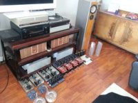
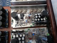
multiple gold'''''' clones pics
so here is whats keeping me up at night these winter months....
only missing small parts ....in the mail somewhere
so guess you'll hear from me often when this babies r being powered up
so here is whats keeping me up at night these winter months....
only missing small parts ....in the mail somewhere
so guess you'll hear from me often when this babies r being powered up
Attachments
Hello Liliya, thank you for your reply.
I have also studied the whole thing and arrived to your same result.
1. for some reason I have the Nemesis 3 board with 2 transistor output version. This I obtained directly from Nagys.
2. most of the references of this thread address the nemesis 9 device.
3. the diference between them is 2 more output MOSFET's to make 3 total and increase output power and some changes in drivers and other semiconductors. Also resistors are added with the supply inputs. Capacitors values change. Circuit seems to be identical.
4. the power supply for Nemesis 3 is +/- 40 and +/- 60 VCC ; and is +/- 60 and +/- 80 VCC for Nemesis 9 version. I don't know GN9 power output.
5. most other PCB's use lateral TO-247 devices instead of original TO-3 package.
Now:
1. the protection circuit is included in my PCB in terms of copper and components allocation.
2. I have a neat circuit version that oiphy provided.
3. part numbering DO NOT MATCH mine.
4. don't know yet if the protection circuit is the same in both GN3 and GN 9
5. oiphy is showing a very similar (yet not identical) PCB as mine but it is good for GN9 not for my GN3 circuit. Can't see any ground plane cuts in it.
6. I don't know if oiphy's version is working and if it does, if it works fine.
Would like some help about evaluating this protection circuit and if I should incorporate it in my PCB.
With just a Dremmel drill I think I could make my board be a GN9
Question 1: are the Alex mm boards still avaliable for buying 2 of them ?
Please correct me if I'm wrong.
Thank you very much for your support
Roberto
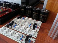
Goldmund clone
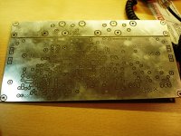
This is a photo of the PCB for Golmund 9.2 that Bigpanda sold. Copare tis with your own (Nagys) PCB
http://www.diyaudio.com/forums/group-buys/175296-pcb-order-goldmun-clone-31.html
I will try to find a copy in my document of the silkscreen of Bigpandas PCB.
Eivind Stillingen
This is a photo of the PCB for Golmund 9.2 that Bigpanda sold. Copare tis with your own (Nagys) PCB
http://www.diyaudio.com/forums/group-buys/175296-pcb-order-goldmun-clone-31.html
I will try to find a copy in my document of the silkscreen of Bigpandas PCB.
Eivind Stillingen
OK Eivind, this is a G3 version similar I think to the one oiphy showed. As the metal is shiny, it is hard to get a good picture, but this one here is very good.
I will compare it to mine but I can tell you that I had done a quick compare of oiphy's layout and it has differences.
It would be nice to hear something about ground planes. Nagys said sometime that Goldmund didn't split planes in any way.
Thank you so much !
Roberto Berner
I will compare it to mine but I can tell you that I had done a quick compare of oiphy's layout and it has differences.
It would be nice to hear something about ground planes. Nagys said sometime that Goldmund didn't split planes in any way.
Thank you so much !
Roberto Berner
- Home
- Amplifiers
- Solid State
- The Very Best Amplifier I Have Ever Heard!!!!